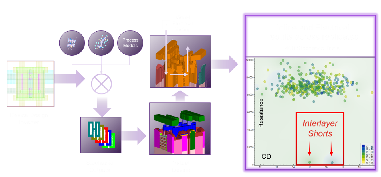
At the recent SPIE Photomask Technology + Extreme Ultraviolet Lithography conference, an expert panel discussed the growing importance of edge placement error (EPE). I had the pleasure of joining moderator Jed Rankin of IBM and fellow panelists Hans Stiepan of Carl Zeiss SMT, Ezequiel Vidal-Russell of Micron Technology, Jo Finders of ASML, Il-Yong Jang of Tekscend, and Vivek Balasubramanian of Applied Materials. Together, we brought perspectives spanning OPC and EDA, mask technology, lithography systems, materials, and metrology. One point quickly became clear: EPE is no longer a narrow lithography metric. It is becoming a system-level measure of how well our industry can translate design intent into a manufacturable, high-yielding device. The mask, scanner, resist, etch process, metrology, OPC, and downstream integration all contribute. Each discipline can optimize its own part, but a collection of local optima does not automatically produce the best device—even if everyone arrives with an excellent slide explaining why their part is already optimized.
As pitch scaling becomes more difficult, tighter control of placement, variability, and pattern fidelity becomes one of the main paths to continued scaling. The challenge is that EPE is an unbounded budget. Mask three-dimensional effects, absorber profile, sidewall angle, critical-dimension uniformity, registration, scanner behavior, resist variability, etch, stochastic effects, process-induced stress, and even wafer or die bonding can all move an edge or change its electrical consequence. Yet the audience survey delivered a wonderfully familiar verdict: OPC was viewed both as a major source of EPE and as the leading place from which future EPE reduction would come.
Source link