This article has been reviewed according to Science X's editorial process and policies. Editors have highlighted the following attributes while ensuring the content's credibility:
Scientists from the Institute of Metal Research (IMR) of the Chinese Academy of Sciences have developed an ordered patterning strategy that integrates p-type and n-type BiVO₄ stripes on a conductive substrate. This strategy enables efficient Z-scheme charge separation and significantly enhances the photocatalytic overall water-splitting process. The research is published in the journal Advanced Energy Materials.
Although solar-driven water splitting is a promising route to green hydrogen, photogenerated electrons and holes tend to recombine, and surface reverse reactions severely limit efficiency. Solid-state Z-scheme heterojunctions connect two semiconductors through a conductive mediator and can provide a high driving force for water splitting while directing high-energy electrons and holes to different components. However, conventional particle-based Z-scheme systems rely on random interparticle contacts, which makes charge-transfer pathways uncontrollable and often exacerbates recombination.
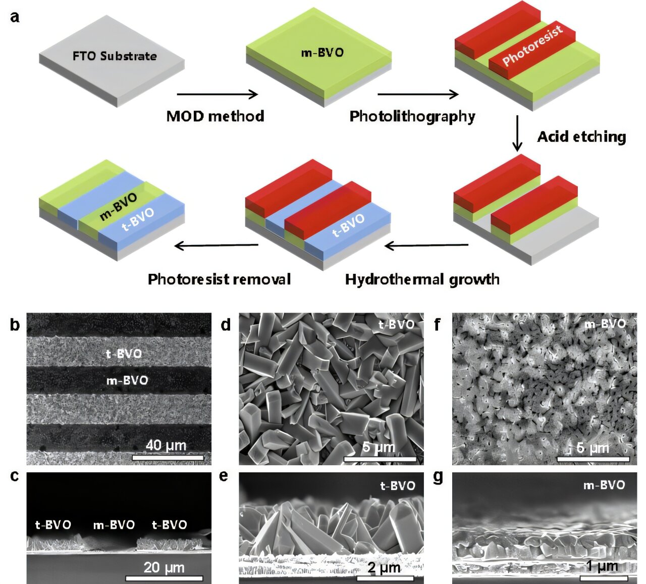
To address this issue, the researchers proposed an ordered patterning strategy. Using photolithography, they fabricated alternating stripes of p-type tetragonal zircon BiVO₄ (t-BVO) and n-type monoclinic scheelite BiVO₄ (m-BVO) on an FTO conductive glass substrate.
The FTO layer serves as a conductive mediator that establishes Z-scheme charge-transfer channels between adjacent stripes. Photogenerated electrons accumulate on the p-type t-BVO stripes and photogenerated holes accumulate on the n-type m-BVO stripes. This spatial separation effectively suppresses charge recombination and reverse reactions.
The patterned panel was fabricated by first depositing an m-BVO film on FTO via metal-organic decomposition, then patterning it by photolithography and wet etching, and finally hydrothermally growing t-BVO epitaxially on the exposed FTO regions.
Source link