Artificial intelligence (AI) and high-performance computing (HPC) are driving unprecedented demand for data movement. As bandwidth requirements climb and conventional electrical interconnects encounter limitations in power consumption, latency and reach, silicon photonics, near-packaged optics (NPO), and co-packaged optics (CPO) are becoming increasingly important technologies for next-generation data centers.
Much of the industry’s attention has focused on photonic device innovation. But demonstrating a high-performance photonic integrated circuit (PIC) is only part of the challenge. Turning these devices into products that can be manufactured reliably and economically at high volume requires a test infrastructure that can keep pace.
This represents a significant shift. Semiconductor manufacturing has benefited from decades of refinement in automated electrical test. Silicon photonics adds an optical dimension that brings new requirements for fiber alignment, coupling efficiency, polarization management, and optical instrumentation—while still requiring conventional electrical characterization.
As silicon photonics moves from development environments toward high-volume production, test becomes more than a quality gate. It is an integral part of the manufacturing strategy.
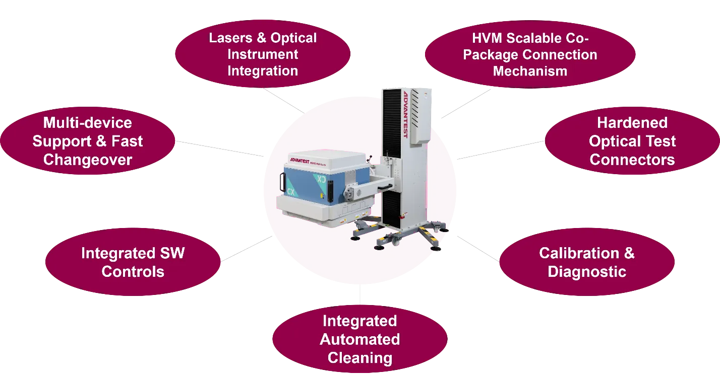
Fig. 1: An HVM-ready test solution requires a full complement of supporting hardware and software.
One of the most fundamental challenges is establishing a reliable optical connection to the device under test. Unlike electrical probing, where physical contact provides a relatively straightforward interface, optical testing depends on precisely coupling light into and out of very small structures.
That coupling must be repeatable from device to device and wafer to wafer. Even small variations in fiber position or angle can affect insertion loss and measured optical performance, potentially making it difficult to distinguish actual device variation from variation introduced by the test setup.
Source link