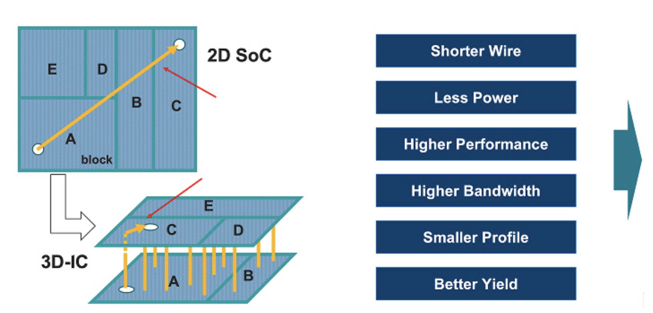
Today’s multi-chip and chiplet solutions are leading the way for the “More than Moore” vision, with companies leveraging packaging technologies to create value and differentiate themselves from their competitors. Through-silicon via (TSV), wafer-level packaging (WLP), and 3D stacking technologies offer a wide range of packaging options for all form factors. Figure 1 illustrates a common example of 3D die/wafer stacking vs the traditional 2D system-on-a-chip (SoC).
As semiconductor packaging technologies such as chip-on-wafer-on-substrate with redistribution layer (CoWoS-R) and local silicon interconnect (CoWoS-L) increase in complexity due to the rapid growth in the number of signals and the integration of high-bandwidth memory (HBM), high-speed interface areas are a key focus for design and analysis. This complexity challenges traditional design and analysis workflows, as importing large designs into analysis tools and managing redesigns can exceed project time constraints, making it difficult to meet deadlines.
This white paper presents a comprehensive methodology that enables early and iterative optimization of IC package designs. By integrating in-design analysis (IDA) directly into the design environment and leveraging scalable multiphysics simulation engines, IC package engineers can compress design cycles, reduce late-stage surprises, and achieve confident sign-off on complex advanced package designs.
Source link