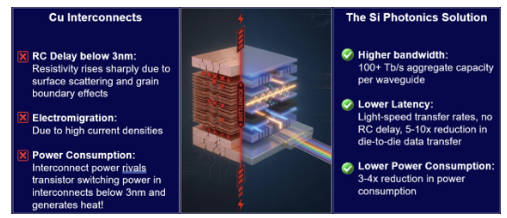
These are three of the challenges facing manufacturers as AI pushes electrical interconnects toward their limits. Silicon photonics (SiPh) and co-packaged optics (CPO) offer a path forward by using light to transmit data rather than relying solely on electrical signals. But realizing those benefits at production scale introduces another challenge: maintaining precise process control across the optical structures, materials and integration processes that ultimately determine device performance and yield.
At the same time, traditional copper interconnects face increasing resistance, electromigration and power challenges as semiconductor architectures scale (Figure 1). For manufacturers, the shift toward silicon photonics places greater importance on precise control of optical structures and materials.
Fig. 1: In the AI era, interconnects (within die and die-to-die and board-to-board) become the bottleneck. Source: Onto Innovation
One of the fundamental differences between conventional semiconductor manufacturing and silicon photonics is what manufacturers need to control.
Photonics yield and performance depend on critical dimensions and tight control of geometry, films and defects. Optical performance can be highly sensitive to relatively small process variations, with consequences for device performance and yield.
Fiber connect (V-groove) geometry, which can affect fiber placement, alignment and coupling efficiency.
Waveguide geometry and cladding, where height, width, sidewall roughness and taper, refractive index and cladding thickness influence light confinement and propagation, along with defects located on the waveguide facet itself.
Microlenses, where defects, shape, placement and material nonuniformity can degrade transmission, beam shaping and coupling.
Die attach, die level bow/warp, micro bumping, through silicon vias (TSVs) and related integration structures, where geometry and defects can affect optical and electrical performance.
Source link