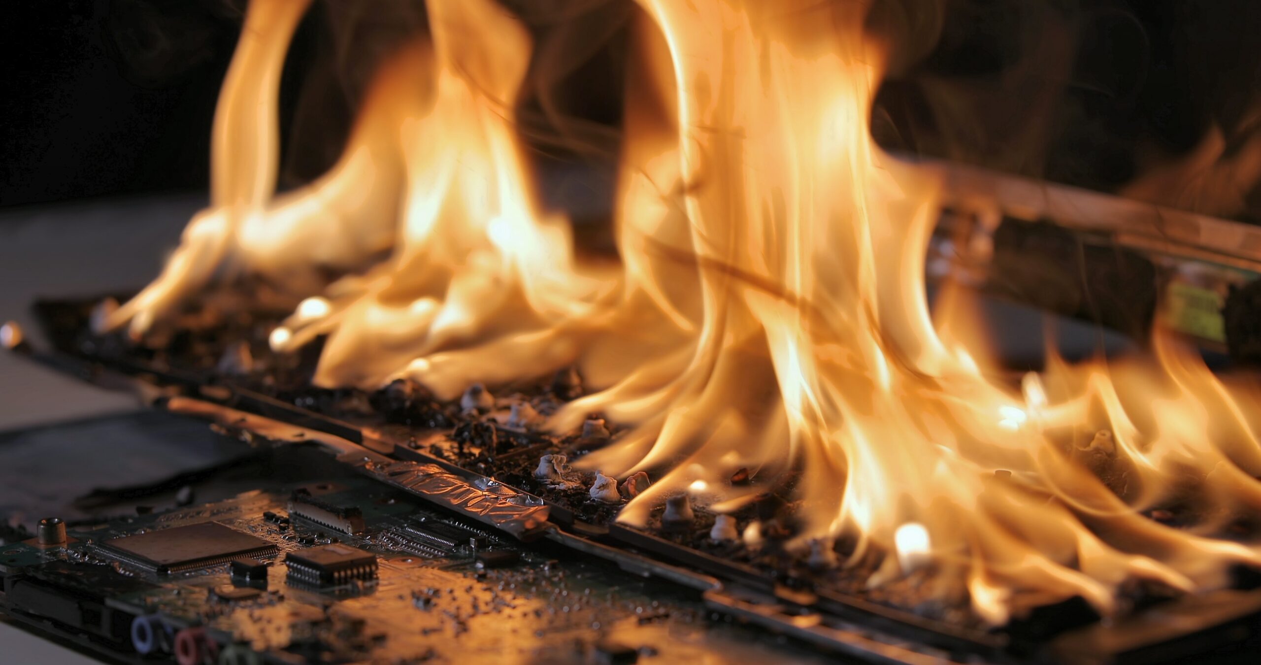
AI, high-performance computing and advanced semiconductor packaging have pushed power density higher, and that means managing heat is becoming one of the most consequential challenges in electronic design.
The issue is no longer simply how to cool a chip after it has been designed. Thermal behavior now affects decisions spanning device performance, package architecture, mechanical stress, reliability, floor planning and ultimately system performance. So engineering teams must shift thermal analysis to earlier in the design process as they consider a much broader multi-physics strategy.
Traditionally, engineers could isolate and analyze many physical effects separately. Electrical performance could be evaluated in one environment, thermal behavior in another and mechanical stress in another and so on. But with increasing integration, a change intended to improve performance in one domain can create unintended consequences elsewhere. Higher power can increase temperature; temperature can change electrical behavior; and thermal expansion can introduce mechanical stress that ultimately affects reliability.
This is particularly worrisome when it comes to chiplets, 3D-ICs and other advanced packaging architectures. Multiple dies, interconnects, substrates, materials and cooling approaches interact within a tightly integrated structure. Designers need to understand not only what happens within an individual die but how the entire assembly behaves as a system.
And addressing this means examining both accuracy and scale. The engineer developing a chip may need detailed information about localized behavior and potential hotspots. A package engineer needs a different level of abstraction, while a system architect may need to evaluate thermal and performance tradeoffs across an even larger environment.
Source link