Dave Plummer, former Microsoft engineer and wizard of Task Manager, Windows Pinball, and now TMOG, has an interesting project in his hands once again. After seeing exactly how many zeros were in the price tag for a megabyte of memory for his vintage PDP-11, he decided to take matters into his own hands and conjure up a new RAM board.
The PDP-11 is from 1970, and later models could fit in as much as four megabytes of memory. Plummer enlisted the help of ChatGPT and the EasyEDA online circuit simulator, though he notes that he hadn't done complicated projects like this before. As several PDP-11 models used Q-Bus boards for main system components, he designed this RAM as a standalone card, then tested it on a backplane alongside another board containing the system's M8190 CPU.
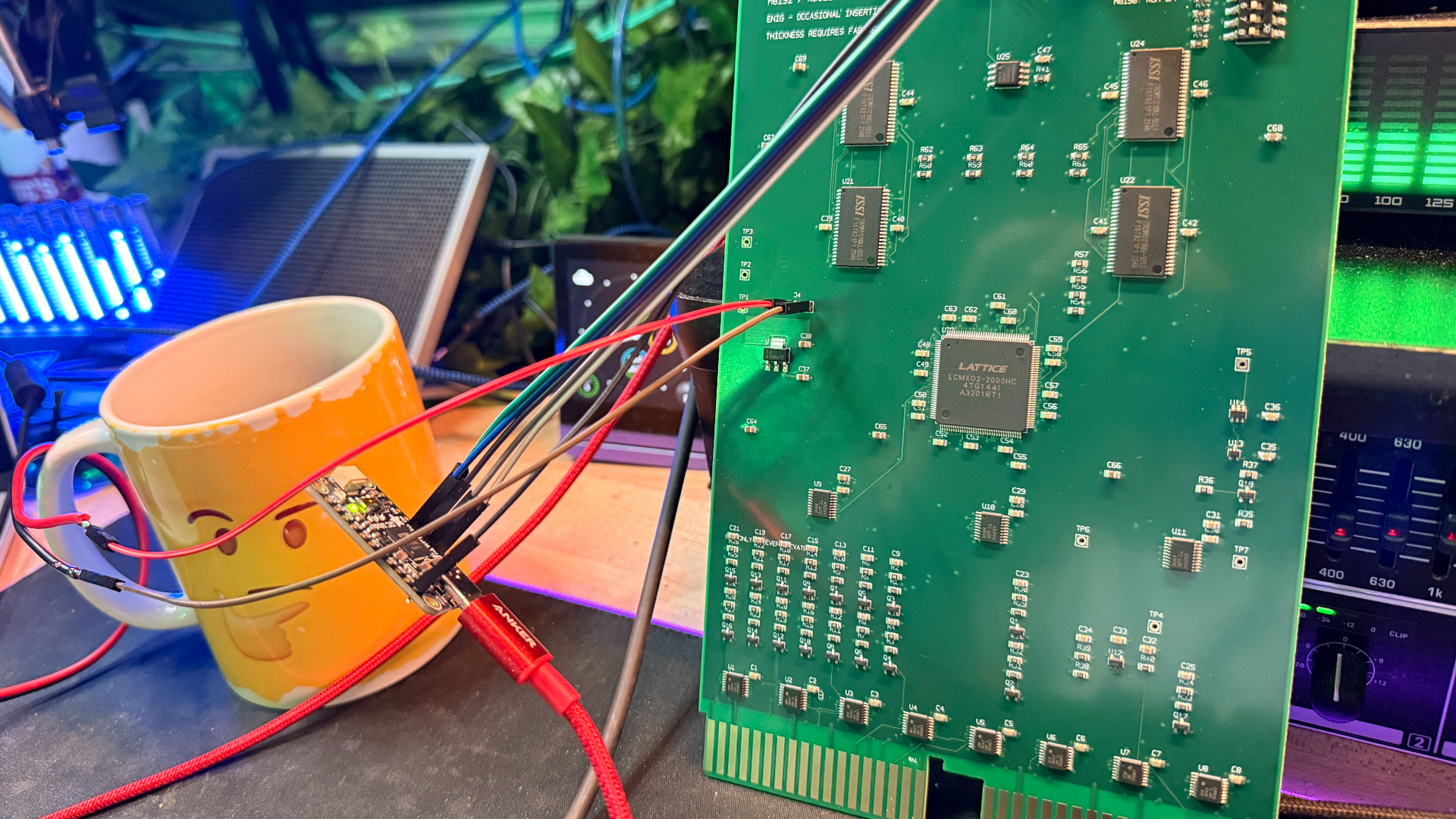
Atop it, he placed a Lattice MachXO2 FPGA serving as a memory controller (model 2000HC, if you're wondering), connected to four ISSI 1 MB memory chips. After adding a U2S I/O chip, a bank of DIP switches, comm ports, and sprinkling a handful of capacitors, he had a complete circuit. The M8190 board design has a 22-bit bus and reserves the top 256 KB for I/O and ROM.
However, it wasn't a first-time-lucky project. Plummer encountered a few abortive starts, as he'd never flash-programmed an FPGA chip before. He fixed that after a few attempts, but then he fell into what appears to be a classic PDP-11 trap.
The machine's memory bus design means it can only access entire words (two bytes) at once, and treats the lowest bit in a memory address as a "lane" selector that picks between the low or high byte in the word.
Source link