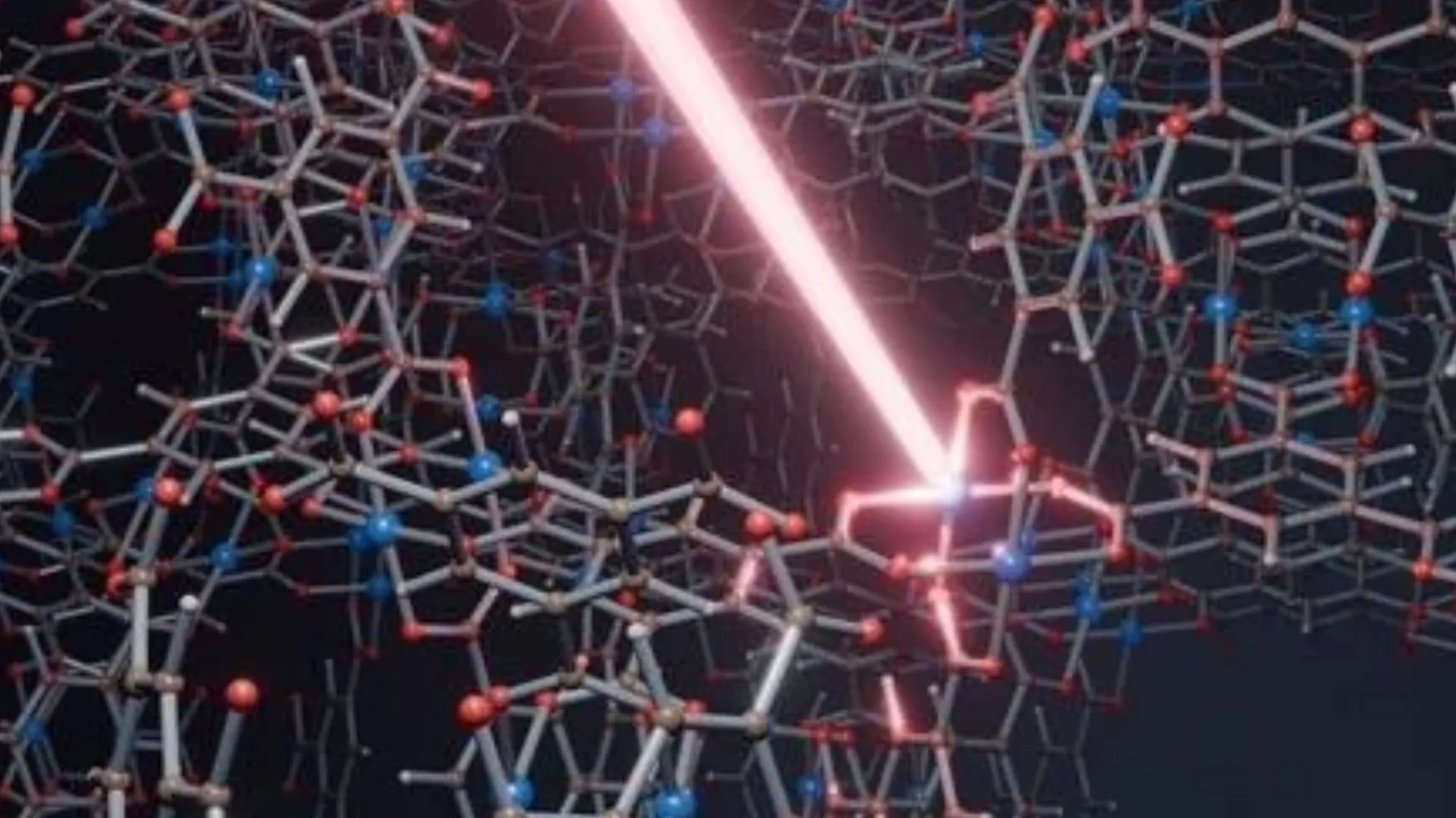
Researchers at the Tokyo University of Science have developed a method to shape porous materials called metal–organic frameworks (MOFs) into microscopic patterns without destroying delicate structures.
Previously, carving these materials into tiny components for advanced electronics or chemical sensors required expensive liquid-nitrogen cooling to prevent them from collapsing under energy beams.
Liquid ionic filler soaks into the MOF’s microscopic pores, strengthening the structure so it can absorb heat and clear electrical charges during standard room-temperature etching.
This low-cost, scalable technique makes it much easier to incorporate over 100,000 known MOF variations into practical technologies like high-sensitivity sensors and micro-catalysts.
Scientists building microscopic electronics have faced a major challenge: their best raw materials crumbled under the tools meant to shape them.
Now, a team of Japanese researchers has unlocked a way to sculpt these delicate crystals using a technique as simple as filling a sponge with liquid.
MOFs are widely considered important for modern materials science. Discovered in 1974 by Professor Richard Robson at the University of Melbourne, these custom-engineered materials link metal ions with organic molecules to create hyper-porous structures.
Imagine a microscopic cage where a single gram offers thousands of square meters of internal surface area. The material’s tiny pores can store gases, trap environmental pollutants, and catalyze complex chemical reactions.
Engineers have long eyed MOFs for next-generation chemical sensors and micro-electronics. Translating that potential into practical hardware required carving the material into precise micro-scale patterns.
Standard semiconductor manufacturing relies on dry etching, blasting materials with high-energy ion beams to strip away microscopic layers.
Source link