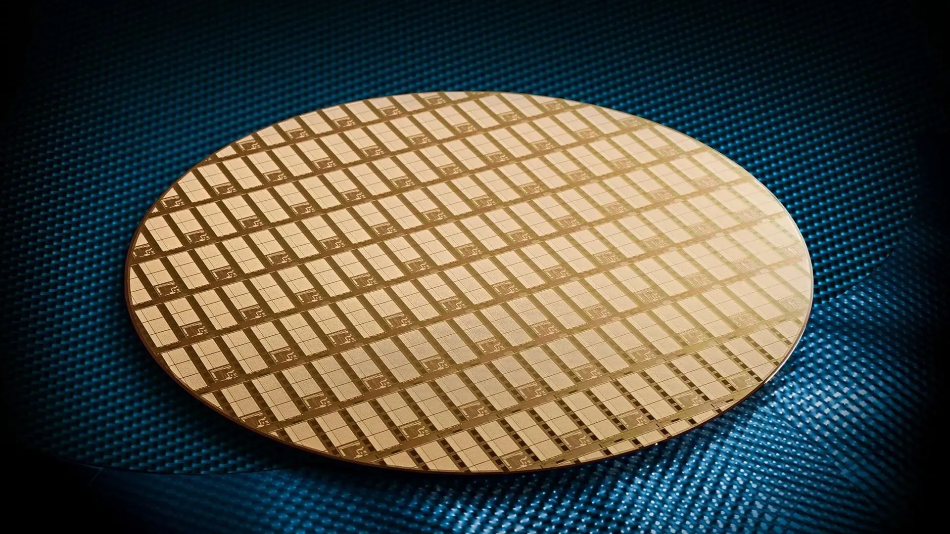
Researchers in South Korea have developed a semiconductor manufacturing technique that controls where individual crystals form with more than 99% success across 400 patterned growth regions, potentially helping manufacturers build vertically stacked computing chips.
The technique allows researchers to grow a single crystal of molybdenum disulfide (MoS₂), a semiconductor only a few atomic layers thick, at a predetermined position instead of allowing multiple crystals to form randomly.
A team led by the Korea Advanced Institute of Science and Technology (KAIST), working with UNIST, Hanyang University and TDS Innovation, developed the method using oxygen released from an oxide barrier to control where crystal growth begins.
The researchers say the approach could address a major obstacle in manufacturing stacked chips, where semiconductor layers must be formed precisely on top of existing circuits without introducing defects that affect performance.
Conventional semiconductor growth methods can define the general area where a thin film forms, but controlling the exact starting point of each crystal remains difficult.
When several crystals grow independently and meet, they create grain boundaries. These boundaries disrupt the regular arrangement of atoms and can interfere with the movement of electrons through the semiconductor.
The researchers developed a process called etching-flux-mediated single-centered nucleation (EF-SCN). Nucleation is the initial stage of crystal formation, when atoms begin arranging themselves into an ordered structure.
The process uses an oxide barrier, such as hafnium oxide (HfO₂), surrounding the designated growth region. Oxygen released from the barrier acts as an etching agent, suppressing unwanted crystal formation.
The oxygen’s effect is strongest near the edges of the patterned region and gradually weakens toward the center.
Source link