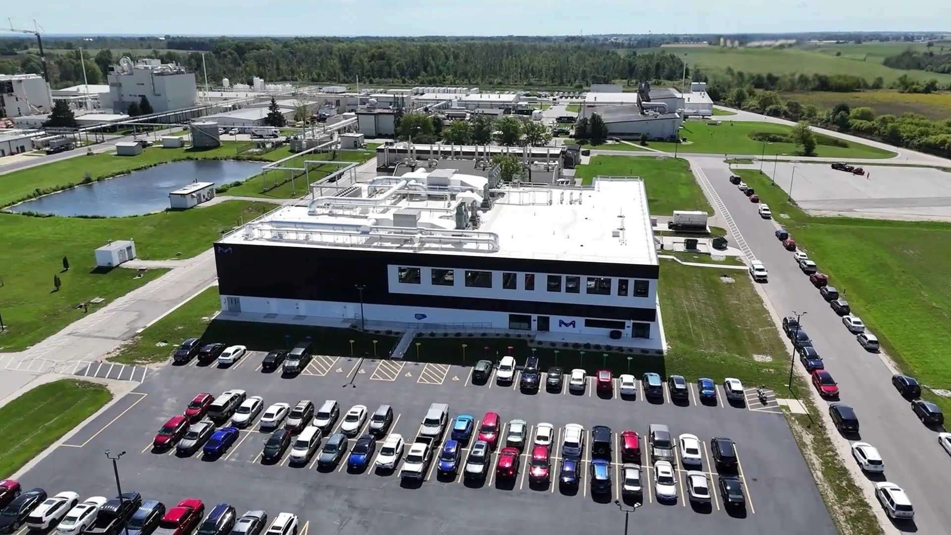
EMD Electronics, the North American electronics business of Germany’s Merck KGaA, has opened a 38,000-square-foot research center in Wisconsin with eight laboratories designed to develop materials for next-generation semiconductor manufacturing.
The Sheboygan Falls facility is part of a $200 million multi-year U.S. investment covering semiconductor operations in Wisconsin, California and Oklahoma. Another expansion at the Wisconsin site is scheduled for completion in 2027.
The new center brings material synthesis, development, scale-up and technology transfer into one location. EMD says the setup is designed to shorten the process of moving new materials from laboratory development toward customer testing and eventual commercial production.
Advanced chips increasingly rely on specialized materials and chemical processes as manufacturers pack more components into smaller spaces and adopt more complex device designs. EMD supplies the semiconductor industry with products including specialty gases, deposition materials, planarization chemicals and patterning materials.
The facility’s eight purpose-built laboratories cover different stages of the product development cycle, including discovery, development, qualification, analytical development, purification, packaging and hazard testing.
Bringing those functions together could allow researchers to develop a material, determine how to manufacture it at larger volumes and prepare the production process for transfer without relying on separate facilities. EMD says this will also allow it to work more closely with semiconductor customers as their manufacturing requirements change.
“The semiconductor industry is entering a period where integrated workflow solutions play a defining role in enabling the next generation of devices, particularly as AI drives increasing complexity and performance requirements,” said Bing Han, executive vice president and head of Thin Films at EMD Electronics.
Source link