Improving power conversion efficiency and long-term operational stability remains a key challenge for perovskite solar cells, partly due to the thermal instability of conventional molecular contacts. Under thermal stress, single-component molecular contacts can lose their ordered molecular packing, compromising hole transport and accelerating device degradation. To address this issue, researchers in China have developed high-entropy molecular contacts (HE-MCs) designed to improve both device efficiency and operational stability.
“Developing high-entropy packing in hole-selective self-assembled molecule (HSM) systems to prevent molecular contact (MC) collapse remains unexplored,” the researchers said. “The key challenge is balancing ordered HSM self-assembly with high-entropy structural complexity while maintaining efficient hole transport.”
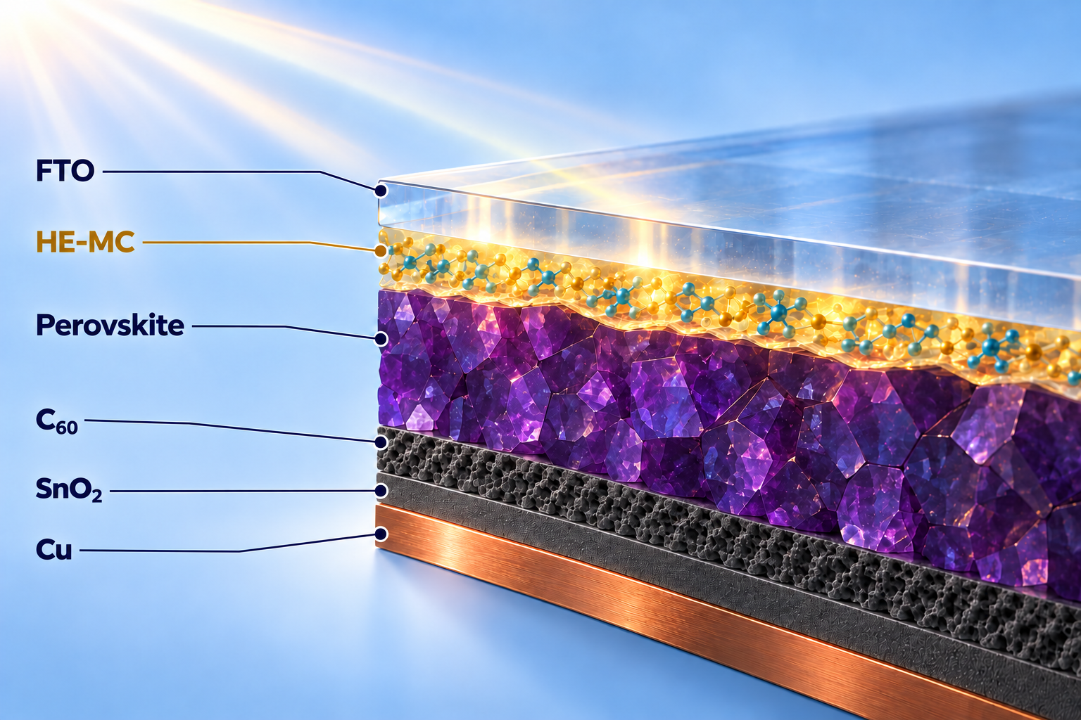
The researchers said their approach involves blending several specially designed HSMs with similar chemical structures but non-centrosymmetric units to promote complex molecular stacking. Mixing the molecules increases configurational disorder and enables the formation of HE-MCs at the hole-selective interface.
The group fabricated inverted perovskite solar cells using a molecular contact consisting of three related carbazole-based molecules: CbzNaph, CbzNaphBF and CbzNaphBT. The latter two incorporate oxygen- and sulfur-containing units, respectively, resulting in different intermolecular interactions and packing arrangements.
The researchers mixed the molecules at a 1:1:1 molar ratio, spin-coated the solution onto cleaned fluorine-doped tin oxide (FTO) glass substrates, and annealed it at 100 C for 10 minutes to form the hole-selective contact.
55 eV using a two-step spin-coating process with chlorobenzene as an antisolvent, followed by annealing at 100 C for 30 minutes. After surface passivation, they deposited a 30 nm fullerene (C60) layer by thermal evaporation, a 40 nm tin oxide (SnO2) layer by atomic layer deposition, and a 100 nm copper rear electrode by thermal evaporation.
Source link