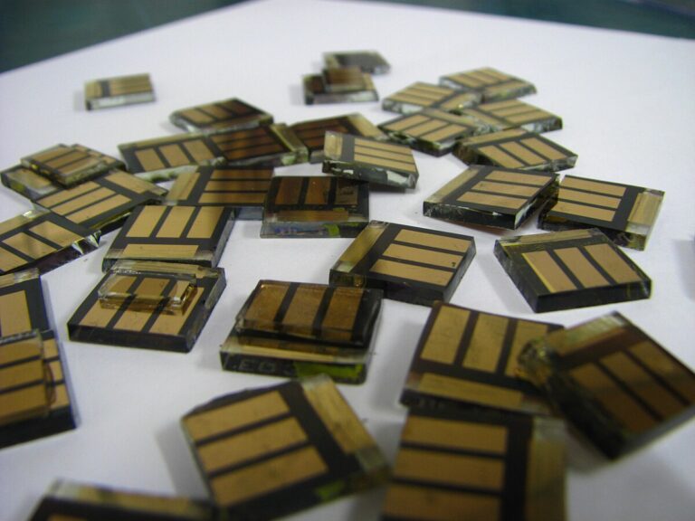
Researchers led by the Huazhong University of Science and Technology modeled lead flows from perovskite photovoltaics in China from 2026 to 2060. They found that, under best-practice conditions, cumulative lead leakage could be up to 94% lower than from crystalline silicon modules using lead-based solder at the same installed capacity.
The study combines dynamic material flow analysis with freshwater ecotoxicity modeling. It tests four perovskite scenarios (business as usual, cleaner production, technology advancement, and best practice) against two silicon cases, with and without lead solder, and assumes perovskites reach 20%, 40%, or 60% of the market by 2060. The researchers used an AI forecasting model to project China’s cumulative PV capacity, reaching about 6,781 GW by 2060. They normalized results by both installed capacity and electricity output, and reported the same relative reductions under each.
The comparison reflects both differences in lead content and assumptions about leakage during manufacturing, use, and end-of-life management. Data compiled by the researchers put single-junction perovskite modules at about 2 grams to 3.9 grams of lead per kilowatt, and all-perovskite tandems at about 3.6 grams to 4 grams, against about 36 grams to 53 grams per kilowatt for silicon modules with lead solder.
In the 40% market-share scenario, cumulative lead leakage from 2026 to 2060 reaches about 479 metric tons under the perovskite best-practice scenario, against about 8,554 metric tons for silicon with lead solder. Under business as usual, perovskite leakage reaches about 2,406 metric tons, more than the roughly 1,848 metric tons modeled for silicon with lead-free solder.
Source link