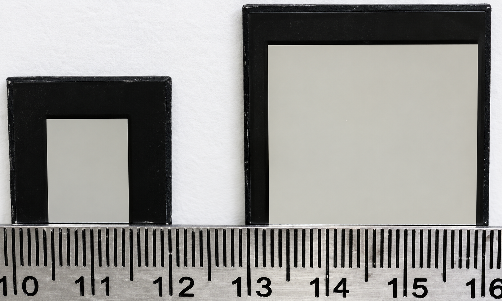
Researchers at the Indian Institute of Technology Bombay have fabricated a large-area inverted perovskite solar cell based on a mixed self-assembled monolayer (SAM) that improves perovskite film quality, enhances charge transport, reduces interfacial recombination losses, and increases device efficiency and stability.
SAMs have emerged as key components in high-efficiency perovskite solar cells, particularly in inverted architectures, where they serve as ultrathin hole-selective contacts that improve charge extraction and reduce interfacial recombination losses. Previous research has shown that SAMs can also enhance device stability and mechanical reliability, while optimizing energy-level alignment between the perovskite absorber and the underlying electrode. More recently, scientists have developed co-assembled SAM strategies to improve surface coverage, suppress defects, and promote better perovskite crystallization. Further advances in SAM molecular engineering have enabled efficiencies approaching 27%, highlighting their potential for developing efficient, stable, and scalable perovskite solar cells.
“We have developed a mixed-carbazole-based SAM strategy for wide-bandgap perovskite solar cells, targeting both surface wettability and suppression of non-radiative recombination at the buried interface. By combining different carbazole-based SAMs, we were able to tune the interfacial properties and promote improved perovskite film formation for the scalabilty of device,” corresponding author Dinesh Kabra told pv magazine. “The impact of the mixed-SAM interface on perovskite film formation and charge-carrier recombination was systematically investigated using morphological and optical characterization.”
1 cm² to larger areas remains a major challenge, particularly for inverted (p-i-n) architectures with wide-bandgap (WBG) absorbers. Although significant efficiency improvements have been achieved in small-area devices, increasing their size typically results in substantial performance losses.
Source link