As the semiconductor industry pushes deeper into the sub-5nm realm, the physical design landscape has shifted from being dominated by gate delays to being defined by interconnect performance. In modern system-on-chip (SoC) designs, the wiring that connects billions of transistors has become the primary bottleneck for power, performance, and area (PPA). Among the various components of the interconnect stack, vias – the vertical connections between metal layers – represent one of the most significant points of vulnerability.
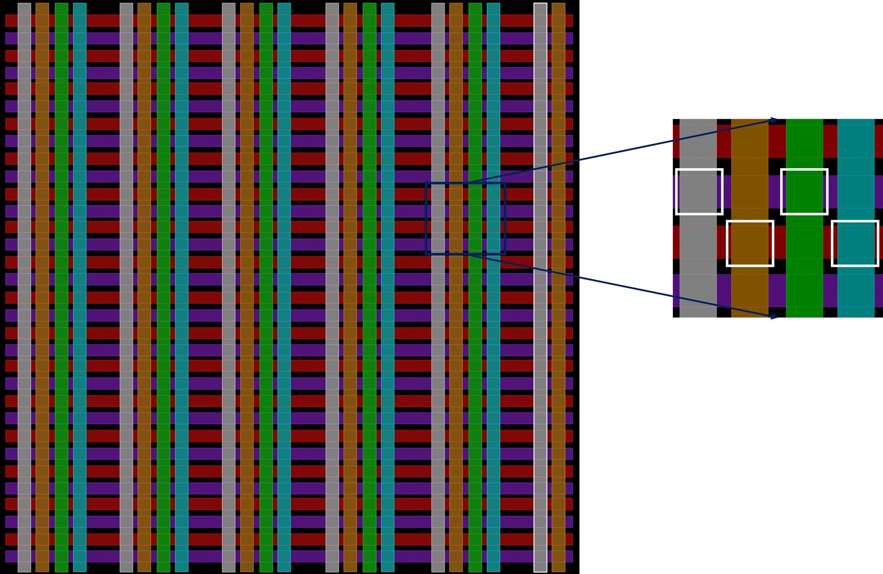
At advanced process nodes, via resistance increases exponentially as dimensions shrink. This rising resistance, coupled with higher current densities, exacerbates challenges related to electromigration (EM) and IR drop. Traditionally, design teams addressed these issues during the final signoff phase, often resulting in late-stage engineering change orders (ECOs) that could delay a project by weeks. To maintain aggressive time-to-market schedules while ensuring long-term silicon reliability, a new approach is required: shifting signoff-aware interconnect optimization into the implementation phase.
To understand the need for automated via optimization, first consider the physical challenges at play. In a typical advanced-node interconnect, the resistance of a single via can be significantly higher than that of a corresponding length of metal wire. As current flows through these narrow vertical structures, the resulting heat and atomic displacement can lead to electromigration – the gradual movement of metal atoms that eventually creates voids or shorts.
Plus, the cumulative effect of via resistance across a massive power delivery network (PDN) leads to IR drop. If the voltage reaching a logic gate falls below a certain threshold, the gate’s switching speed slows down, potentially leading to timing failures.
Source link