For manufacturers scaling advanced AI packages, pressure is mounting from every direction.
While on another, AI packages are growing larger and integrating more high-bandwidth memory (HBM) and high-performance chips.
And that’s to say nothing of the production teams who face increasing pressure to ramp new processes quickly.
While achieving high yield remains a critical goal, success increasingly depends on how quickly manufacturers can establish stable process conditions and transition from development to high-volume manufacturing (HVM).
Fan-out panel-level packaging (FOPLP) has emerged as an attractive path forward for manufacturers looking to scale advanced packaging production.
Compared with traditional wafer-based approaches, FOPLP can significantly improve substrate utilization while increasing the number of packages produced per substrate. In one study comparison, a 300mm wafer achieved approximately 55% substrate utilization with six packages per wafer, while a 300mm panel achieved 86% utilization with 12 packages per panel and a 510 × 515mm panel achieved 74% utilization with 30 packages per panel. This enables manufacturers to improve manufacturing efficiency and reduce costs per package.
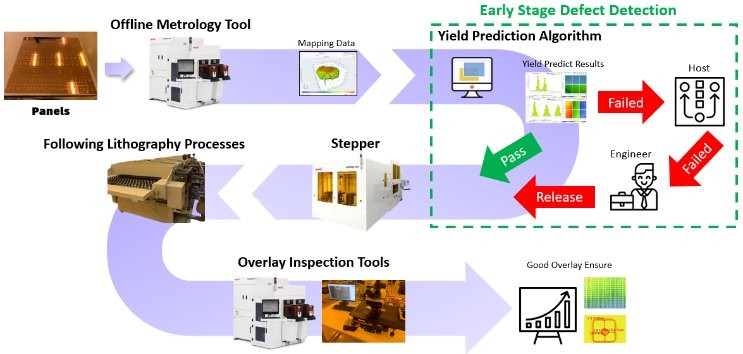
As panel sizes increase, manufacturers must contend with pattern distortion, die shift, and resulting overlay errors across the substrate. These effects directly impact yield and make process optimization substantially more difficult.
Unlike traditional wafer-based processes, panel-scale variation does not behave uniformly. Instead, distortion patterns can vary significantly across the panel, creating localized challenges that are difficult to correct using conventional approaches.
Ultimately, process engineers must identify the “sweet spot” between overlay yield and throughput. To compensate for panel-level distortion, manufacturers typically rely on a range of correction strategies.
Source link