This article has been reviewed according to Science X's editorial process and policies. Editors have highlighted the following attributes while ensuring the content's credibility:
Semiconductor devices such as LEDs and transistors generally consist of two halves: an n-type, which carries negative charge via electrons, and a p-type, which moves positive charge carriers called holes that are essentially electron voids. Both halves rely on contacts that allow electric current to flow in and out with minimal energy loss. These connections, known as ohmic contacts, have been an efficiency bottleneck in thin p-type GaN semiconductors for decades because of their high resistance.
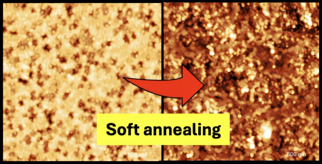
Now, a team led by Haitao Wang and Jia Wang at the Institute of Materials and Systems for Sustainability (IMaSS), Nagoya University, has developed a new way to lower the resistance of p-type GaN contacts. They deposited an ultrathin magnesium layer onto the p-GaN surface and heat-treated it at 600°C (1,112°F) for five minutes, achieving a contact resistivity of (1–3) × 10⁻⁴ Ω cm² without damaging the surface. This is among the lowest reported contact resistivities for thin p-type GaN.
Their findings, which are expected to make a wide range of electronic devices used in places such as electric vehicles and data centers more energy-efficient, have been published in the journal Applied Physics Letters.
Magnesium-doped p-type GaN was developed at Nagoya University by Isamu Akasaki and Hiroshi Amano in work recognized by the 2014 Nobel Prize in Physics for blue LEDs. In this material, holes are produced by adding small quantities of magnesium , which has one fewer valence electron than the surrounding gallium, in a process known as doping.
Source link