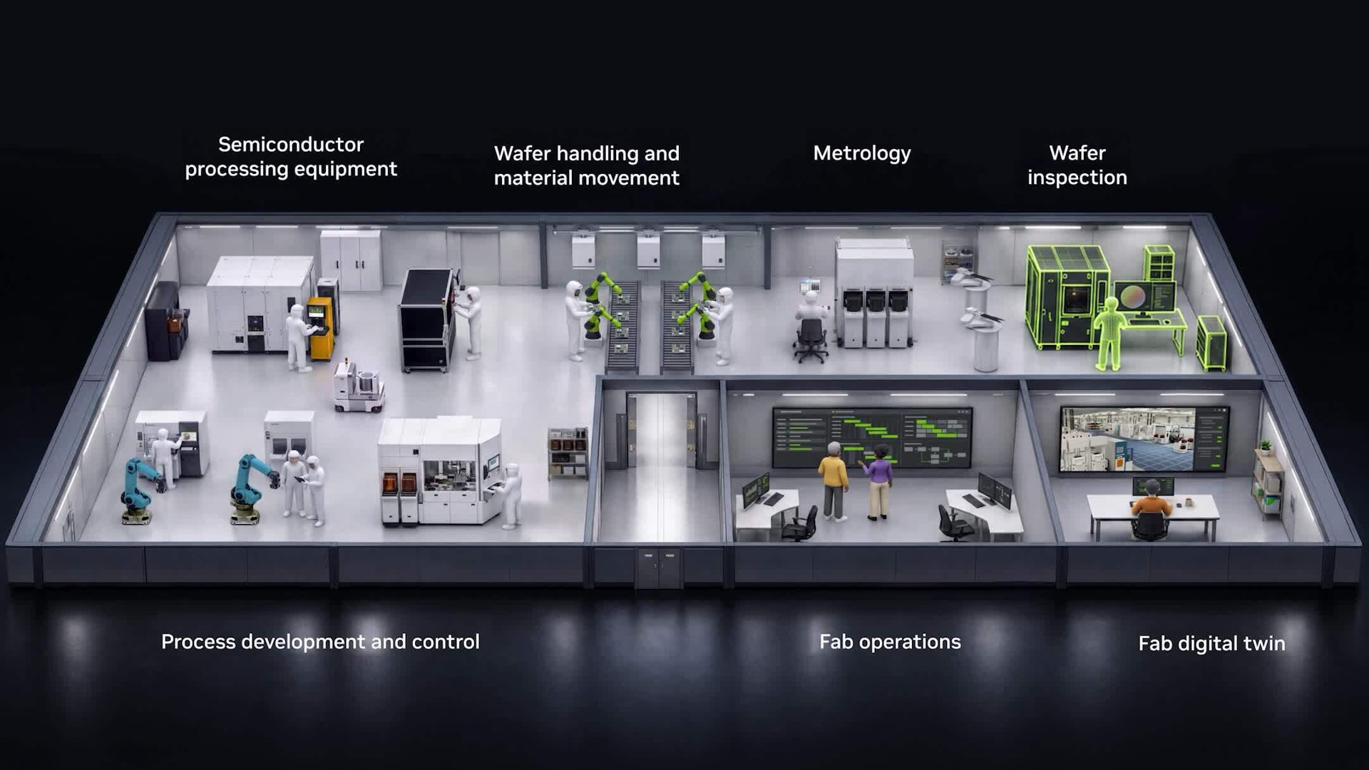
Your browser doesn't support HTML5 video. Here is a link to the video instead.
Demand for advanced chips is rising. The processes to build them are getting more complex. And the margin for error is shrinking.
For engineers, understanding how a process change will behave, how a material will interact with a new step, how a defect maps back to a root cause are critical, challenging steps in semiconductor manufacturing — and these analyses can take days. Physical experiments on a fab line are slow and expensive. A wrong call on yield or process quality has real consequences.
AI is transforming semiconductor manufacturing, impacting what engineers can do — and how fast.
Accelerated computing shortens simulation time, allowing engineers to evaluate more alternatives before committing to physical trials.
Physics-based AI helps engineers predict process behavior without running a full simulation every time.
And digital twins let teams test changes in a virtual environment before committing to physical trials.
Together, these capabilities describe an AI-defined fab: a semiconductor manufacturing factory where AI helps engineers optimize processes, catch problems earlier and make better decisions across the full manufacturing chip lifecycle. Engineers direct the work and make decisions based on their expertise while spending less time waiting for answers.
Accelerated computing doesn’t just speed up individual calculations — it changes how many alternatives engineers can test before committing.
Multiphysics simulations model interactions among physical effects, such as heat transfer, electrical behavior and mechanical stress.
Using the NVIDIA cuDSS library, multiphysics software provider COMSOL is accelerating such simulations for semiconductor manufacturing by up to 10x.
Source link