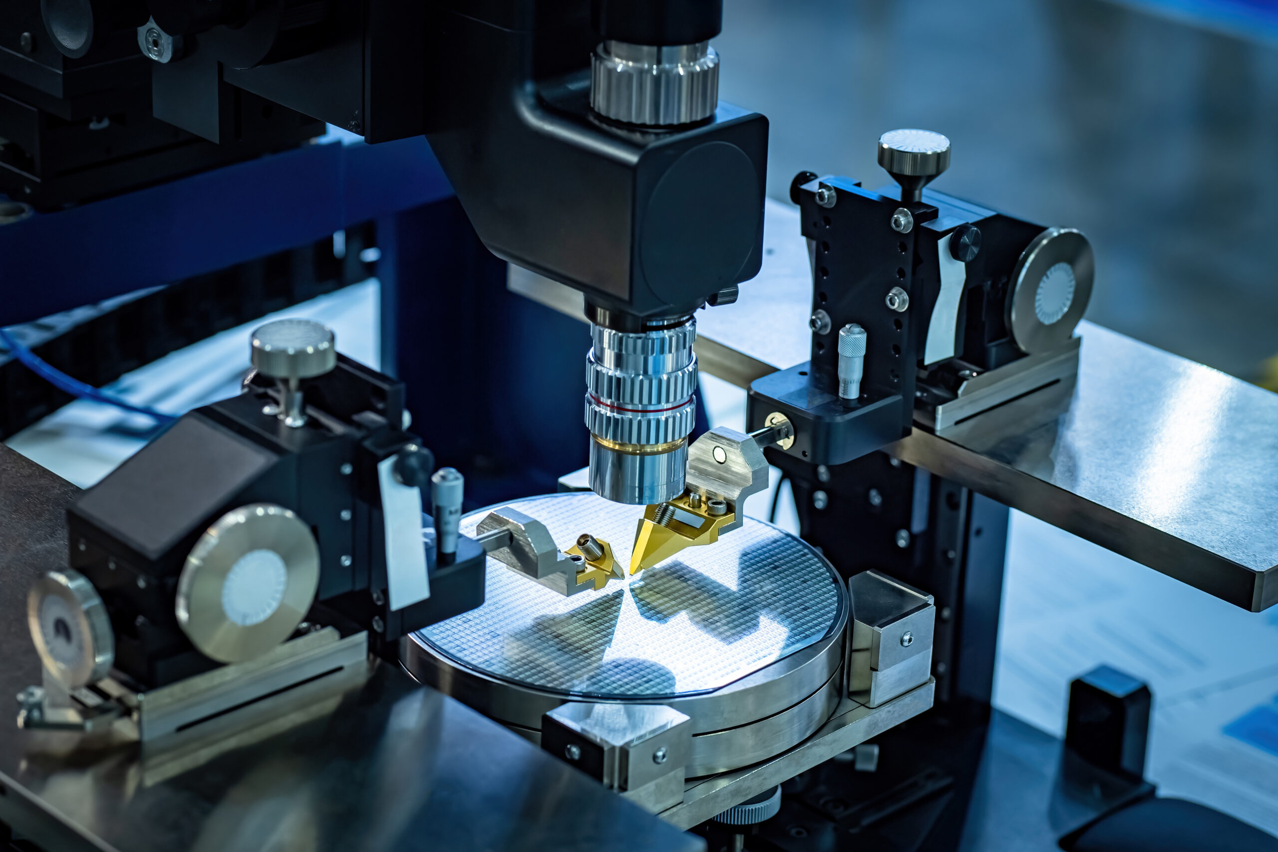
Researchers at Materials Center Leoben, PVA TePla, and Advanced Semiconductor Engineering (ASE) published “AI-Based Image Enhancement Improves Detection of Interconnect Defects in Microelectronic Packaging.”
Abstract Excerpt:
“Traditional failure-analysis (FA) methods face growing challenges due to the increasing miniaturization and complexity of modern semiconductor devices. In particular, the detection of cracks in the extreme low K layers of flip-chips, utilized in advanced packaging architectures at the back end of line (BEOL), is challenging. To improve detectability of these so-called “white bumps”, we propose an AI-based image-enhancement workflow, specifically tailored to improve scanning acoustic microscopy (SAM) images.”
Wilhelmer, R., Djuric-Rissner, T., Czurratis, P. et al. AI-Based Image Enhancement Improves Detection of Interconnect Defects in Microelectronic Packaging. J Fail. Anal. and Preven. (2026). https://doi.org/10.1007/s11668-026-02537-z. Open access.
Source link