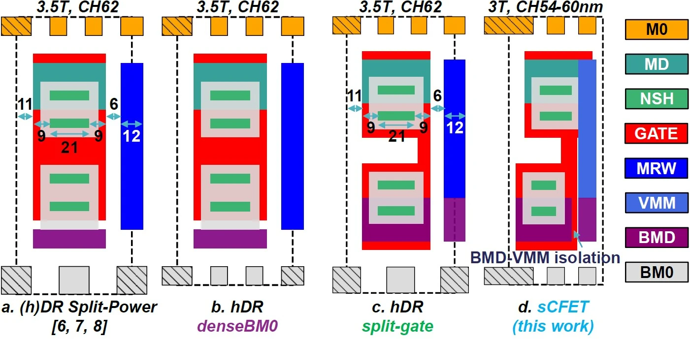
The semiconductor industry is going through a major architectural transition, with gate-all-around (GAA) nanosheet transistors replacing FinFETs in advanced logic nodes of 3nm and beyond. GAA nanosheet transistor technology offers scalability down to the A10 logic generation, where it enables 5.5-track (T) standard cells – the track being a measure for the standard cell height.
For the A7 node, options are becoming increasingly diverse to meet the growing diversification of application needs, driven by the AI revolution. According to imec’s latest roadmap, one option is to design systems around imec’s CMOS 2.0 scaling paradigm. With CMOS 2.0, a system-on-chip (SoC) is partitioned into heterogeneous, functional tiers each optimized using the most suitable technology, and reconnected using 3D interconnect technologies. For other use cases, GAA nanosheet technology may be pushed to its ultimate scaling limits, with power delivered from either the frontside or the backside. But industry may as well transition to complementary FET (CFET) device architectures. By stacking p and nMOS transistors on top of each other, standard cells can be further scaled down to 3T, thereby extending the classical CMOS logic roadmap to at least the A3 technology node.
Imec and its industrial partners are working to make CFET-based devices manufacturable. In recent years, they laid the groundwork for key integration approaches, categorized as monolithic CFET (mCFET) and sequential CFET (sCFET) [1,2].
Both approaches start from the vertical stacking of Si/SiGe layers from which the n and pFETs are fabricated. With mCFET, the vertical device structure with common top and bottom gates is patterned and processed in a single sequence of process steps.
Source link