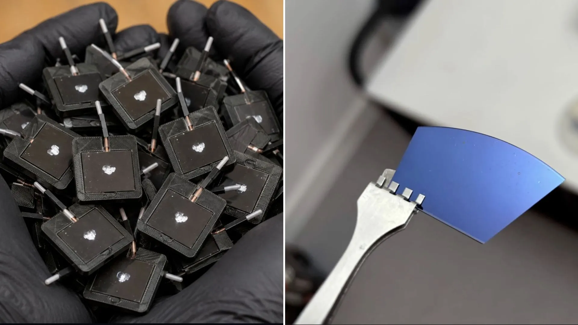
Making a working solar cell usually requires specialized equipment for process silicon, control temperatures, and create microscopic electrical structures. But semiconductor engineer and YouTuber Dr. Semiconductor has demonstrated a more unconventional approach: using a small microwave kiln to turn an ordinary silicon wafer into a functioning photovoltaic cell.
The experiment produced a working cell with a reported efficiency of around 5%, showing that a basic semiconductor device can be fabricated in a home workshop using comparatively accessible equipment.
The result falls well short of commercial solar cells, but the project offers a fascinating look at how silicon’s electrical properties can be modified without a conventional industrial furnace. It also builds on Dr. Semiconductor’s broader effort to demonstrate how semiconductor fabrication techniques can be adapted for a home laboratory.
The central challenge is not simply heating silicon, but creating a junction between two differently doped regions of the semiconductor. That junction allows a solar cell to convert incoming light into electrical energy.
In this experiment, Dr. Semiconductor starts with a p-type silicon wafer, which contains positively charged carriers known as holes. The next step is to introduce phosphorus into the wafer’s surface, creating a thin n-type region. Where the two regions meet, they form a p-n junction that separates electrical charges generated when light strikes the material.
The phosphorus-containing coating is heated using a small microwave kiln. Rather than placing the wafer directly in a microwave oven, the kiln uses a heat-absorbing material to convert microwave energy into heat. The setup reaches temperatures high enough for phosphorus to diffuse into the silicon, a process normally performed using specialized thermal-processing equipment.
Source link