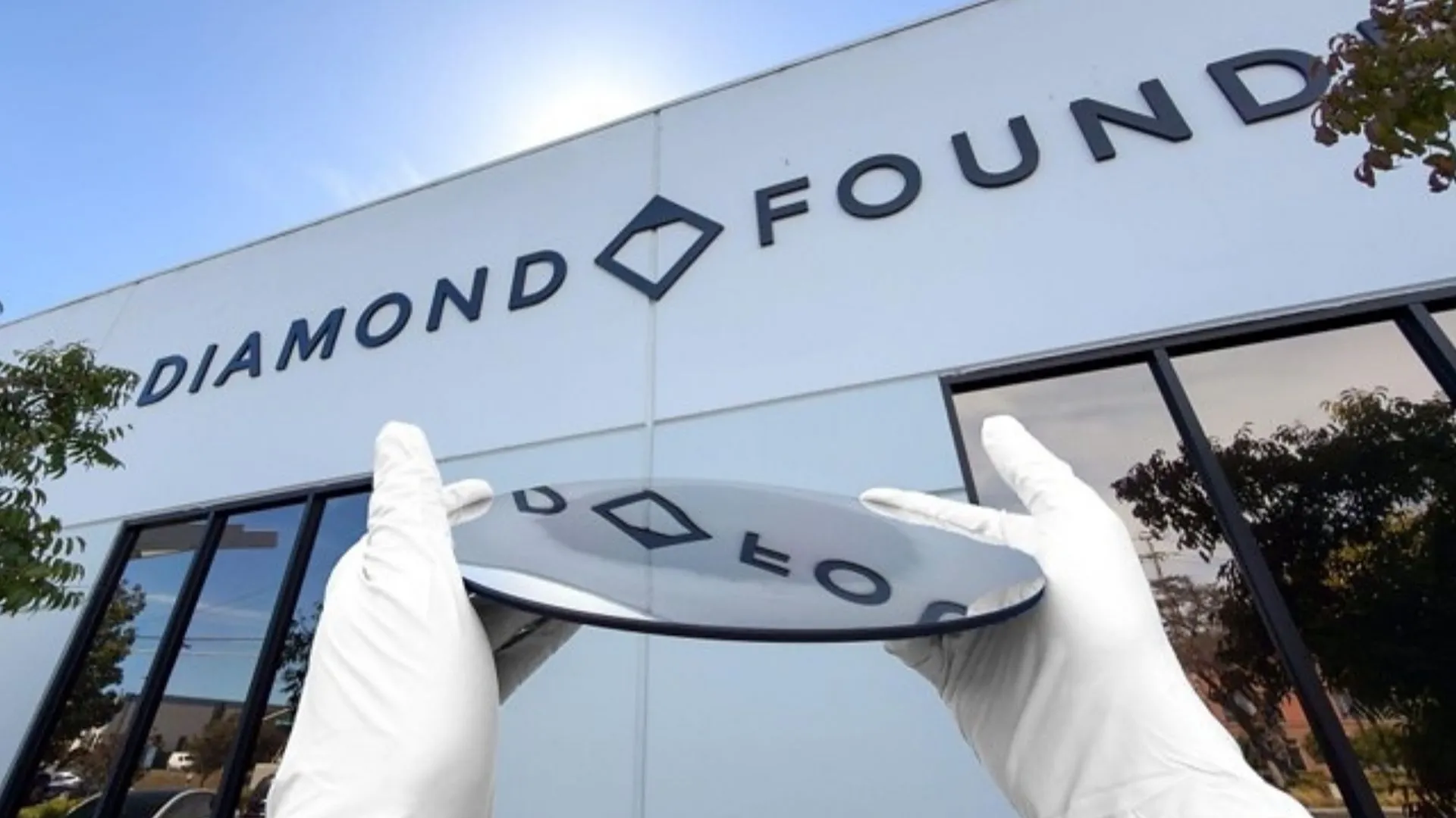
Diamond Foundry says it has produced the world’s first 200-millimeter (7.9-inch) single-crystal diamond, a development that could bring one of nature’s most thermally conductive materials closer to semiconductor manufacturing.
The San Francisco-based company announced the milestone on November 6, describing it as the culmination of a 25-year effort to grow large, continuous diamond crystals.
The achievement is significant because diamond offers a combination of properties that could address some of the challenges facing advanced electronics, particularly the growing difficulty of removing heat from high-performance processors. However, the company has so far shown the new crystal in its as-grown, unpolished state.
The 200 mm crystal is a single continuous structure, rather than a collection of smaller diamonds joined together or a polycrystalline disk containing multiple crystal grains. That distinction matters because grain boundaries and defects can affect how efficiently heat and electrical charge move through a material.
Diamond is made up of carbon atoms arranged in a tightly ordered crystal lattice. Producing a large single crystal requires maintaining that atomic arrangement across the entire material as it grows. Even small inconsistencies can introduce defects that undermine the properties manufacturers want to preserve.
Conventional high-pressure, high-temperature methods can produce synthetic diamonds, but scaling them to semiconductor-sized single crystals presents substantial engineering challenges. Chemical vapor deposition (CVD), which grows diamond from a carbon-containing gas in a controlled environment, offers another route. Microwave plasma CVD is particularly important in research into large, high-quality diamond crystals.
Diamond Foundry’s earlier milestone provides some context. 9 inches) single-crystal diamond wafer produced using diamond heteroepitaxy, a technique that grows a crystal on a different underlying material while encouraging it to adopt an ordered diamond lattice.
Source link