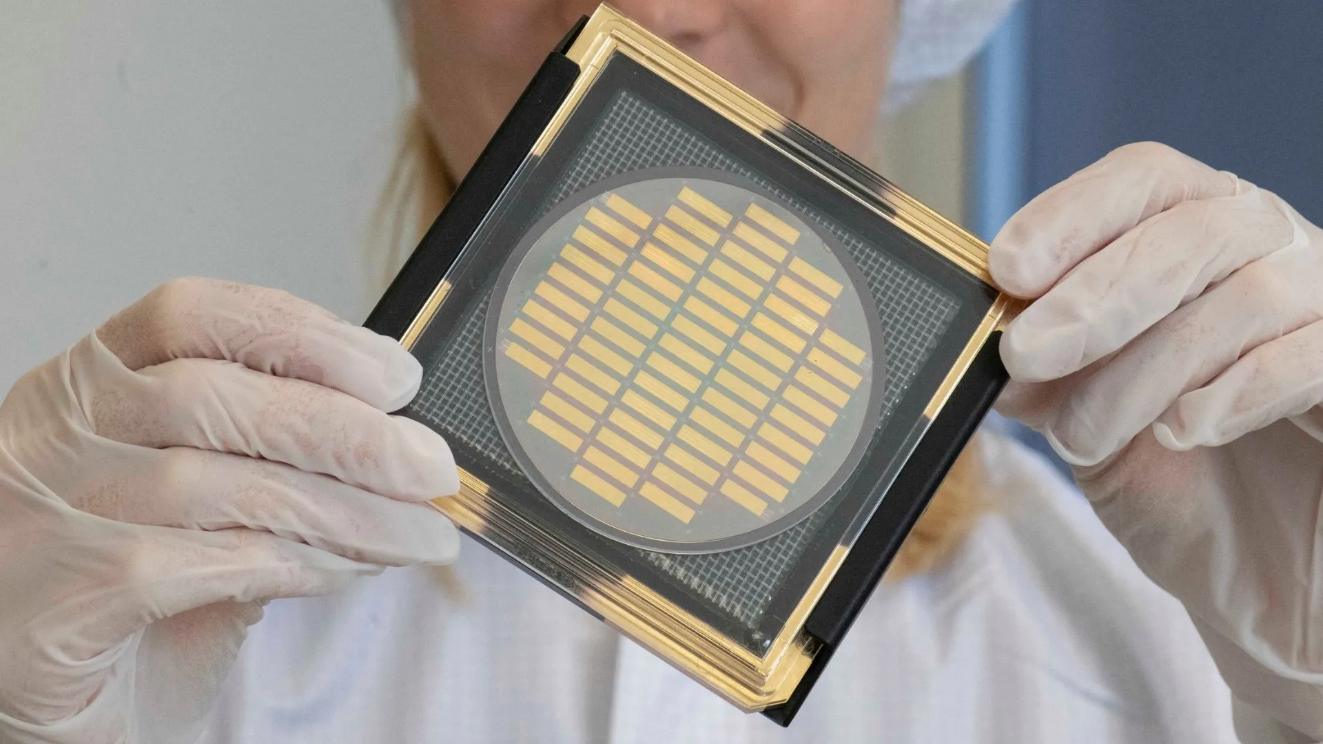
Researchers at Washington University have developed a new method to let silicon photonics efficiently perform the optical functions needed to control and detect light, overcoming a key materials limitation that has restricted their capabilities.
The team at the McKelvey School of Engineering in St. Louis added ultrathin, single-crystal films to existing silicon photonic circuits, with different crystalline materials providing specific functions such as controlling, modulating, and detecting light.
Until now, adding such materials has been difficult because growing them directly on silicon can create compatibility and manufacturing problems. The new method instead grows the crystals separately and transfers them onto the chip afterward.
The materials can be placed side by side or stacked depending on the function required. The team demonstrated light modulation and control, as well as detection across wavelengths ranging from ultraviolet to near-infrared, describing the modular approach as “photonic Legos.”
The team used four materials with different properties to demonstrate the framework. Single-crystalline barium titanate (BTO) provided electro-optic modulation, allowing electrical signals to control light traveling through a chip.
For nonreciprocal light control, the researchers used cobalt ferrite (CFO), which can control how light travels through a device. They also integrated gallium arsenide and gallium nitride membranes on silicon nitride to detect selected wavelengths spanning ultraviolet to near-infrared light.
The researchers went a step further by stacking BTO and CFO nanomembranes on silicon micro-ring resonators, allowing a single device to control light using both electrical and magnetic effects.
“We developed a manufacturing process that will give us more freedom to design these new photonic chips,” said Sang-Hoon Bae, an assistant professor of mechanical engineering and materials science at the university.
Source link