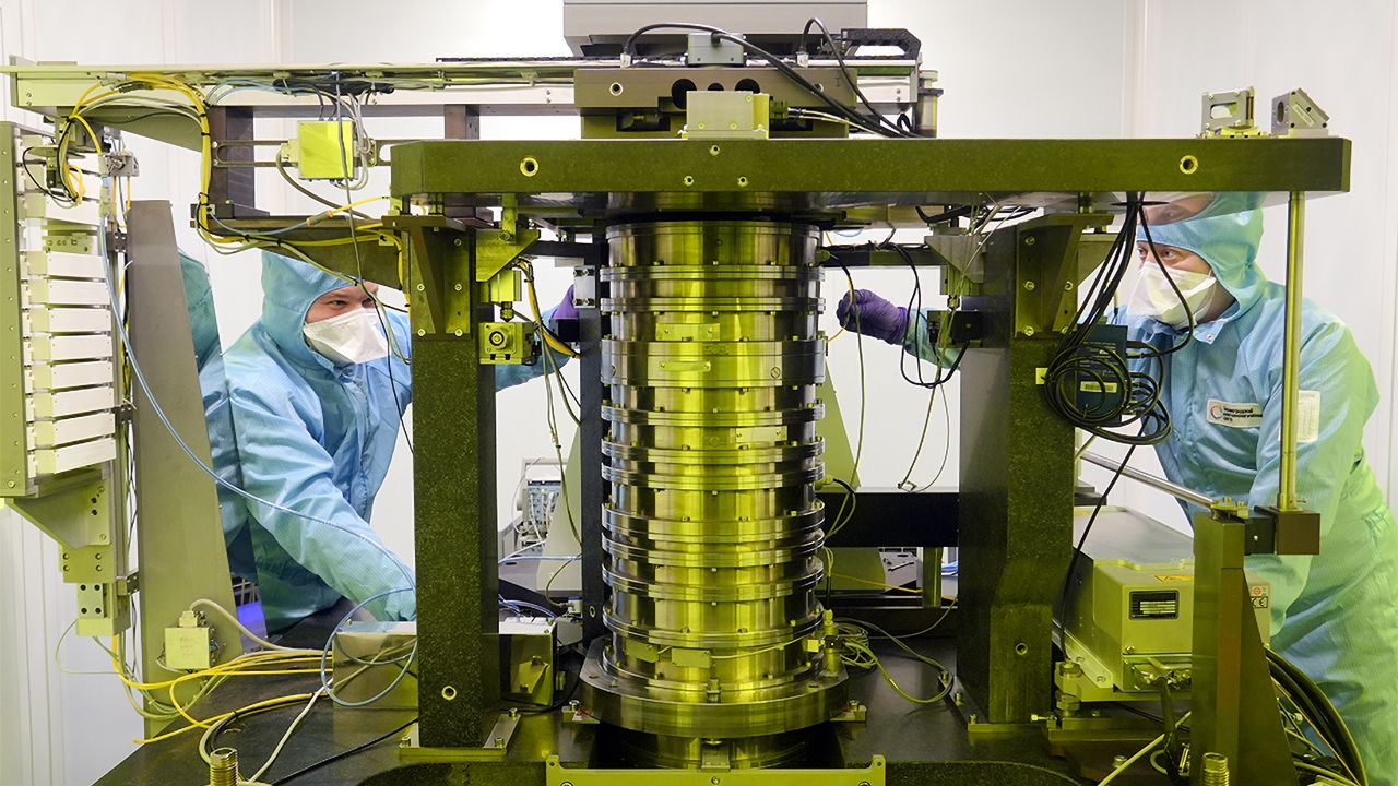
Russia-based Zelenograd Nanotechnology Center (ZNTC) has completed the third R&D stage of the company's first lithography tool capable of processing 200-mm wafers using a 130nm process technology, reports CNews. The tool is currently being tested internally and is years away from being used at a real fab to produce chips in mass quantities. Blogger Dmitrii Kuznetsov suggests that the device is the "first Russian 130nm-capable lithograph" that consists of components made in Russia. This may not be the case, though.
- Photonics and high-speed data movement is the next big AI bottleneck
- Co-Packaged Optics (CPO) foundry roadmaps
- Inside optical and the battle for scale – how the AI industry is racing to integrate photonic interconnects
- How optical interconnects and silicon photonics emerged as AI's next hot commodity
- Near-packaged optics (NPO) gains ground as the industry hedges against CPO's growing pains
"The creation of a prototype of a domestically developed photolithography system designed for a 130nm process is an important milestone for Russia's microelectronics industry," Alexander Mikhailov, an analyst with Strategy Partners, told CNews. "It demonstrates that Russia has its own engineering expertise required to develop such equipment and paves the way for developing a range of systems targeting smaller process nodes (90nm and 65nm)."
Truth be told, while the Zelenograd-based ZNTC is responsible for the project, Belarus-based Planar was responsible for developing the lithography system, according to documents seen by CNews (which corroborates earlier reports ). In addition to the system itself, Planar was responsible for manufacturing mechanical assemblies and components, as well as commissioning the prototype.
Source link