Having jettisoned 4F2 memory cells from its roadmap, Micron must use different methods to continue scaling its DRAM devices in the coming years to keep up with rivals planning to use smaller DRAM transistors towards the end of the decade. Instead, Micron intends to introduce wafer bonding with its upcoming 1ε DRAM process technology and adopt High-NA EUV lithography for subsequent generations. Meanwhile, the company is developing new types of memory, including vertical high-bandwidth memory (vHBM) and vertical edge inference memory (vEIM), which will be integrated directly on top of processors.
- Leading-edge foundry roadmaps
- Nvidia Enterprise GPU and CPU roadmap
- AMD's Enterprise GPU and CPU roadmap
- Intel's roadmaps examined — 14A, Nova Lake, Diamond Rapids & AI accelerator push
- Co-Packaged Optics (CPO) foundry roadmaps
"DRAM is nearing atomic limits at this point," said Scott DeBoer, president and chief technology and products officer at Micron, during the company's event this week. "Although we have confidence in several more planar nodes, we are very focused on making sure that we introduce 3D DRAM at the optimal time from a cost and performance point of view."
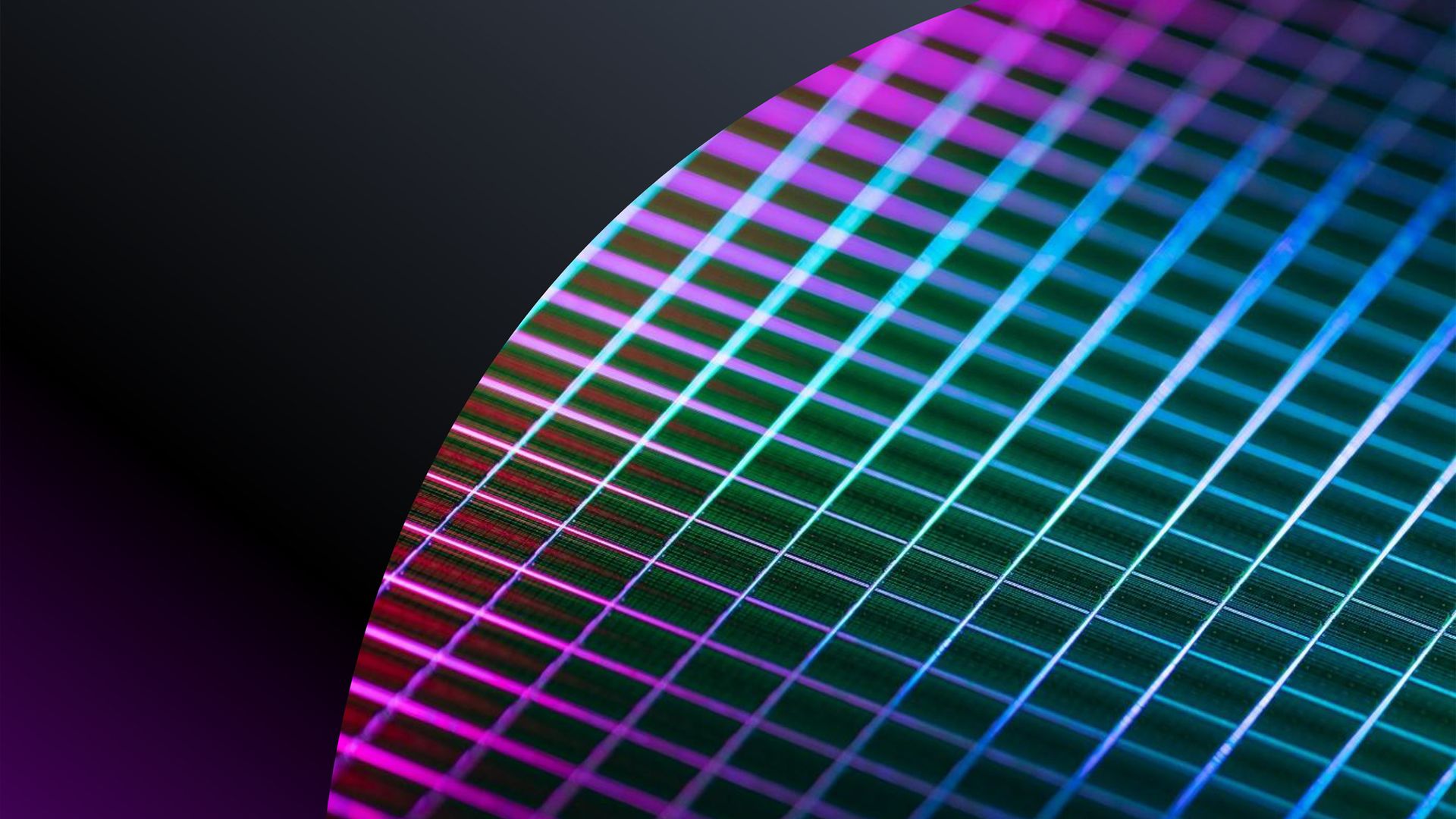
Micron's current 1γ DRAM process is already in high-volume manufacturing, whereas its successor, 1δ, is scheduled to enter volume production in the second half of 2027. The latter promises a mid-20% increase in bit density and is optimized for future AI memory products, including HBM5, vHBM, and vEIM. Beyond 1δ, Micron plans to introduce wafer bonding with its 1ε process, which is currently under development.
Source link