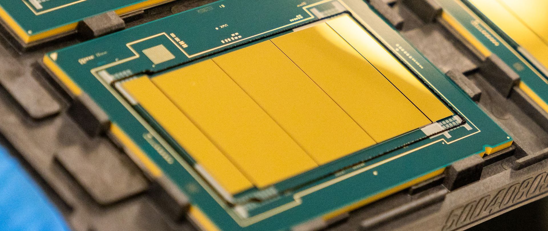
Advanced packaging technologies have become integral parts of advanced CPU and GPU designs, and virtually all of Intel's high-end client and data center CPUs rely on its Embedded Multi-die Interconnect Bridge (EMIB) and Foveros technologies. But what's next for these two advanced packaging methods? Before we try to see where both technologies are going, let's first take stock of where we are today.
Although Intel's advanced packaging saga began in 2017 with the Kaby Lake-G CPUs and Stratix 10 FPGAs, packaging technologies weren't quite the hot topic they are today. However, both Intel and its industry peers were working relentlessly to advance these technologies, so Intel was among the first companies to outline a detailed roadmap for multi-chiplet processors featuring its 2.5D and 3D integration technologies — EMIB and Foveros — back in 2020. Following the fiasco with its initial 10nm process technology, the company made it clear that its multi-chiplet strategy is a sustainable way to deliver performance and feature enhancements cost-efficiently and at a predictable cadence. While we certainly cannot say that all of Intel's multi-chiplet projects were a success, it is safe to say that the majority of Intel's client and data center CPU products launched in recent years use multiple chiplets and rely on EMIB and Foveros advanced packaging technology.
In fact, as Intel's advanced packaging roadmap evolves, EMIB and Foveros not only become more sophisticated to address the demands, but they also become simpler to cover cost-sensitive products. Another peculiarity about Intel's packaging duo is that they no longer seem to be two mostly separate technologies.
Source link