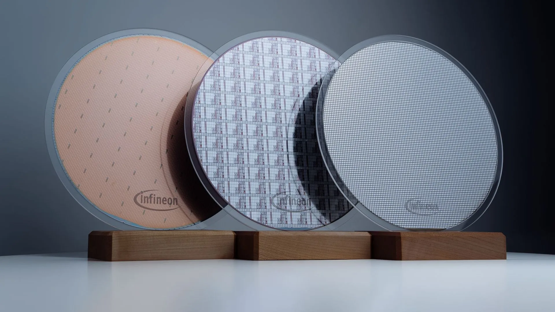
German chipmaker Infineon Technologies has announced that it has made working power chips on 300-millimeter silicon carbide wafers at its plant in Villach, Austria. Announced on November 9, this is a first-of-its-kind attempt made in a full-scale fabrication facility, using equipment already in place for manufacturing silicon chips.
The larger wafers could help Infineon increase its supply of power semiconductors for electric vehicles, renewable energy systems and AI data centers.
The company said a 300-mm wafer can yield 2.3 times as many chips as a 200-mm wafer. It is showcasing a processed wafer at the electronica trade show in Munich, which runs from Nov. 10 to 13.
The work in Villach established that Infineon could use existing silicon production equipment to turn the larger silicon carbide wafers into functional devices.
The company plans to work with customers and partners on the technology and the timing of a production ramp-up. It will also continue developing its 200-mm silicon carbide manufacturing process.
“This technological milestone further strengthens our leadership in power systems. Congratulations and thank you to our passionate team, making significant progress in bringing 300-millimeter SiC out of the lab into a manufacturing environment,” said Jochen Hanebeck, CEO of Infineon Technologies.
Silicon carbide is the second wide-bandgap material in Infineon’s 300-mm manufacturing plans, alongside gallium nitride.
On October 27, the company announced an investment of about €1.1 billion in a high-volume facility in Villach to make gallium nitride power semiconductors on 300-mm wafers.
Infineon also tested its Cold Split process on 300-mm silicon carbide at its Dresden, Germany, site.
Source link