We all know how important inspection is for advanced packaging. Not only are these processes critical for ensuring higher yield, but they’re also integral for maintaining device reliability. As the industry pushes for smaller features and tighter spacing, even the smallest defects can pose major challenges. For instance, delaminations and air gaps can be detrimental in a market that demands increasingly complex devices. Such defects will lead to electrical or mechanical failures down the road.
One technology that’s mitigating these issues is acoustic micro imaging (AMI). AMI is a high-frequency ultrasound technology, and it’s being used by the industry as an inspection method.
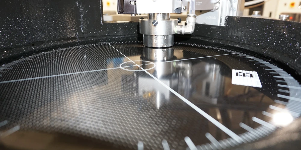
At the core of AMI technology is a transducer, or a device that turns energy from one form to another. It starts with a pulse of electrical energy, then converts it to mechanical energy, or a high-frequency ultrasound wave. Because ultrasound doesn’t travel through air, this allows inspectors to obtain clear images of gaps and delaminations in the device that could otherwise be difficult to see.
However, the transducers used for AMI are not all the same. Each transducer handles a specific frequency, and they’re chosen based on the sample that needs to be inspected. By moving the transducer across the sample, the inspector can generate multiple images that can then be analyzed by the AMI software. Through this analysis, the inspector can choose to accept or reject parts based on the number of defects the package is found to have.
The biggest difference between ideal and defective samples is that some defective samples will have very clear air gaps.
Source link