This article has been reviewed according to Science X's editorial process and policies. Editors have highlighted the following attributes while ensuring the content's credibility:
A research group from the Hefei Institutes of Physical Science (HFIPS) of the Chinese Academy of Sciences (CAS) has developed a method for manufacturing flexible films that can effectively shield electromagnetic waves across a broad frequency range. The films can be produced on a square-meter scale.
"This means we can make thin materials that protect electronic devices from electromagnetic interference," said professor JI Shulin from the Institute of Solid State Physics at HFIPS, who led the research.
The relevant findings were recently published in ACS Applied Materials & Interfaces and Langmuir.
With the growing use of electronic devices and communication technologies, electromagnetic waves are increasingly common in everyday environments. However, conventional materials for absorbing or shielding these waves often need to be thick to work effectively and typically cover only a limited frequency range. This makes it difficult to develop thin, flexible films that provide broadband protection.
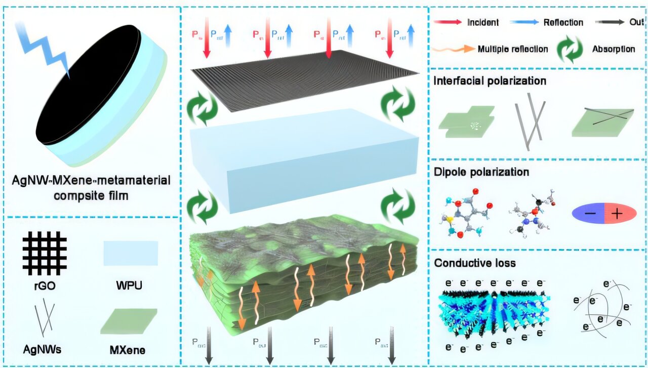
In this study, the researchers introduced a design called cross-dimensional percolation, which combines nanomaterials of different dimensions into a three-dimensional interconnected network. By adding precisely printed conductive patterns, known as metastructures, the researchers enabled the films to regulate electromagnetic waves across a wider range of frequencies.
The researchers also developed a manufacturing process combining pressure-assisted filtration, precision inkjet printing, and transfer techniques. They improved the films' flexibility by modifying their surface chemistry and developed a conductive ink to ensure accurate printing of the metastructures.
Source link