AI is entering the inner loop of semiconductor engineering by reducing the effort required to develop software, operate software tools and carry out engineering analysis.
Ray Kurzweil described the broader pattern as the Law of Accelerating Returns: accumulated technical capability helps create the next computing paradigm. In my recent white paper, The semiconductor singularity: Accelerating IC innovation with AI, I applied that idea to semiconductor engineering. Better computing improves the tools used to design and manufacture semiconductors, and those tools help create the next generation of computing.
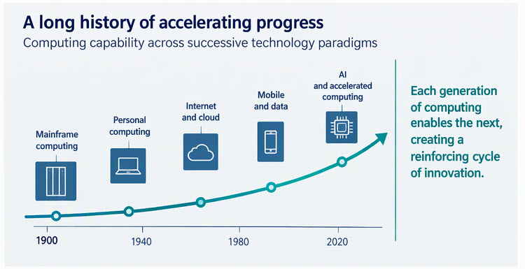
Figure 1 places that loop in the longer history of computing. The technologies change, but each generation contributes tools, knowledge and capacity that help create its successor.
Fig. 1: Successive computing paradigms have built the technical capacity used to create the next generation.
Progress in semiconductor engineering never follows a smooth exponential curve. It advances when a bottleneck is overcome sufficiently for engineers to try something that previously cost too much money, time, computation or organizational effort.
I saw this firsthand with machine learning in computational lithography. Early demonstrations were exciting, but production adoption required developers who understood both ML and semiconductor applications, representative data, model management, IP controls and customer confidence. Production adoption followed only after the model, data, deployment environment and customer requirements matured together.
Generative AI relieves many of the user-complexity bottlenecks characteristic of EDA flows. When I created my original SPIE machine-learning course for lithography, the prototype work took roughly 200 to 300 hours, including some help generating training data.
Source link