This article has been reviewed according to Science X's editorial process and policies. Editors have highlighted the following attributes while ensuring the content's credibility:
Just as carbon atoms arranged in different ways can form either graphite or diamond—the hardest natural material—semiconductor materials can also exhibit completely different properties depending on their atomic arrangements. Now, a previously overlooked crystal structure of indium selenide (In2Se3) has been brought to life as a promising material for next-generation logic electronics.
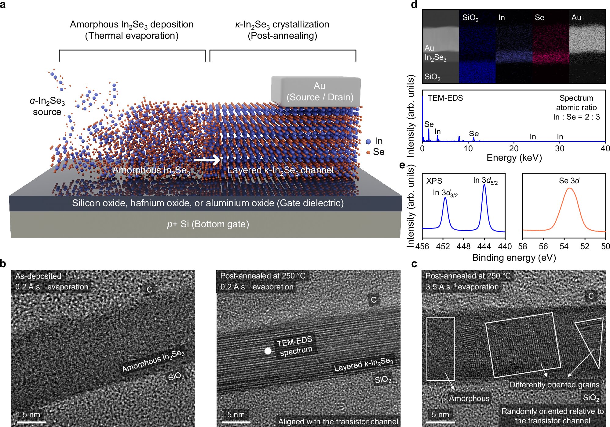
A research team led by professor Yong-Young Noh from the Department of Chemical Engineering at POSTECH, including graduate student Jaeyun Lee, in collaboration with professor Jimin Kwon and Dr. Yongwoo Lee from the School of Electrical Engineering at KAIST, has developed wafer-scale logic transistors based on the rarely explored κ-phase In2Se3.
In2Se3 has long been considered a promising next-generation semiconductor material because of its atomically thin structure and excellent charge transport properties. However, previously studied crystal phases have shown limitations.
Their ability to retain a previous electrical state after voltage removal—known as a "memory effect"—is beneficial for memory applications but can cause instability in logic circuits that require identical outputs from identical inputs. In addition, although high performance has been demonstrated in small exfoliated flakes, achieving uniform and high-quality In2Se3 films over large wafer areas has remained a major challenge for practical semiconductor manufacturing.
The research team turned their attention to the previously underexplored κ-phase In 2 Se 3 .
Source link