This article has been reviewed according to Science X's editorial process and policies. Editors have highlighted the following attributes while ensuring the content's credibility:
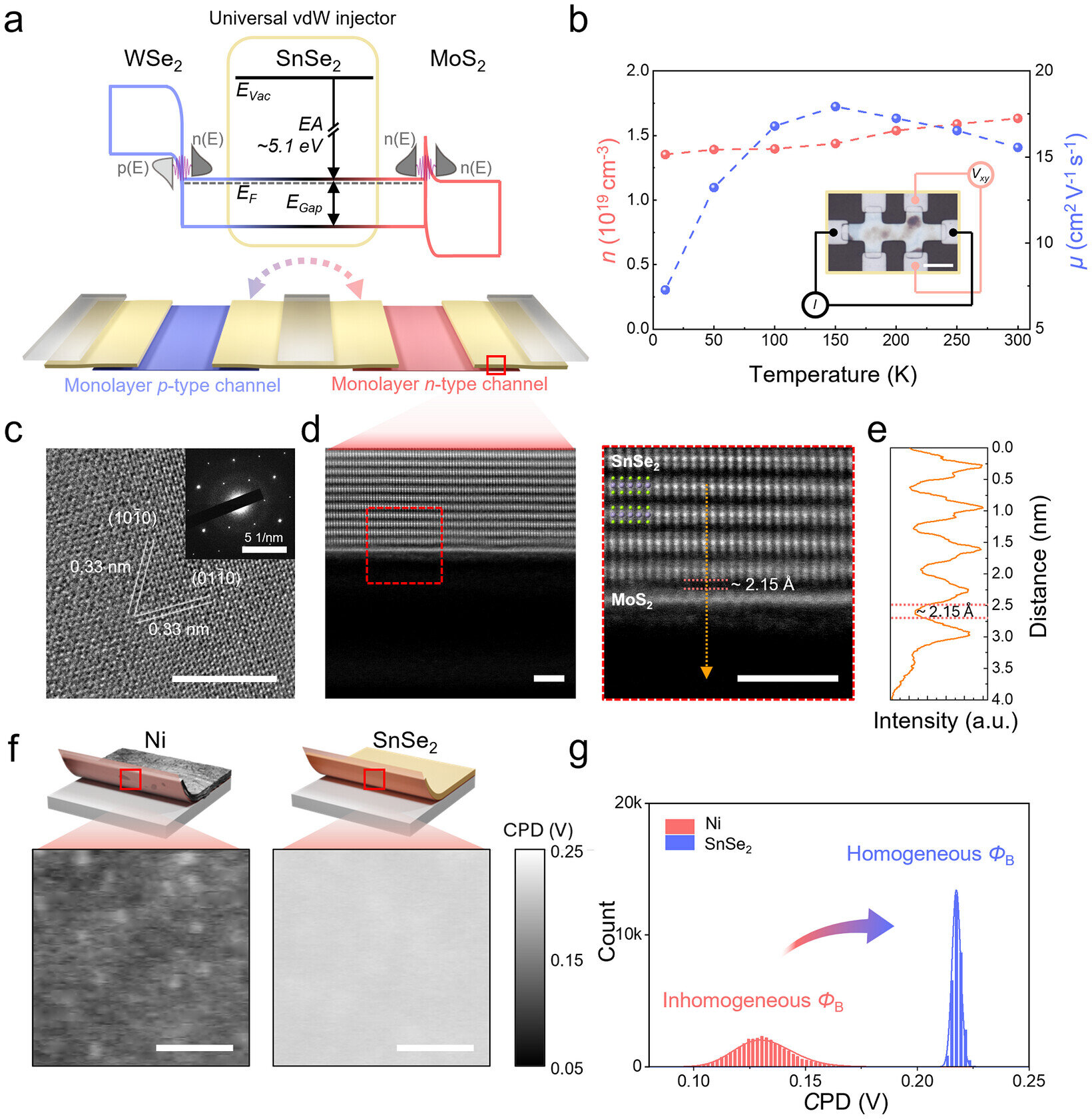
A new approach could help make future AI chips smaller and more energy-efficient. A KAIST-led research team has used a single material to address one of the major obstacles facing atomically thin semiconductors: the difficulty of efficiently injecting charge. The technology could contribute to next-generation AI and low-power semiconductor devices in which multiple ultrathin layers are vertically integrated to increase device density and performance.
A research team led by Professor Joonki Suh from the Department of Chemical and Biomolecular Engineering developed a "universal van der Waals tunneling injector" based on tin diselenide (SnSe2). The single-material injector efficiently supplies charge to two different types of atomically thin semiconductor channels.
The study was conducted in collaboration with researchers from Yonsei University, the Beijing Computational Science Research Center in China, the Korea Institute of Science and Technology (KIST), Hanyang University, the Ulsan National Institute of Science and Technology (UNIST), and Samsung Electronics.
A transistor is a microscopic switch that controls the flow of electric current. Nearly every semiconductor chip, from those used in smartphones and computers to advanced AI processors, contains vast numbers of transistors.
Transistors can be broadly classified as n-type or p-type. In n-type transistors, "electrons" carry the current, while in p-type transistors, current is carried by "holes," which are empty electron states that act as positive charge carriers. Modern semiconductor chips combine these two types in complementary metal-oxide-semiconductor, or CMOS, circuits, which enable fast operation while minimizing power consumption.
Source link