This article has been reviewed according to Science X's editorial process and policies. Editors have highlighted the following attributes while ensuring the content's credibility:
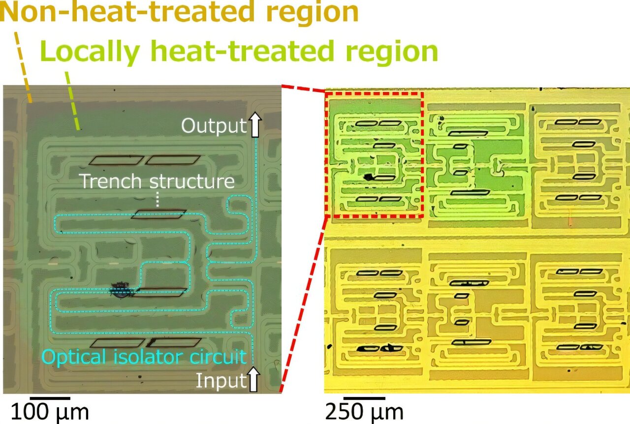
Kyocera Corporation and the Research Institute of Electrical Communication (RIEC) at Tohoku University have developed a new technology that integrates optical isolators directly onto silicon photonics chips using laser annealing, a method that applies localized heat treatment using a laser.
As generative AI and other data-intensive technologies continue to expand, data centers need to process more information while using less energy. Silicon photonics can help by using light to transmit data efficiently. Silicon photonics is also important for Co-Packaged Optics (CPO), which combine optical and electronic circuits in the same semiconductor package to shorten signal paths, reduce signal loss and lower power consumption.
However, in optical circuits, some light can be reflected back toward the laser source, reducing performance. Optical isolators help prevent this by allowing light to travel in only one direction.
As optical circuits become smaller and more integrated, there is growing demand for optical isolators that can be fabricated directly onto silicon photonics chips.
These isolators typically use a crystalline material called magneto-optical garnet, which must be heated to 600°C (1,112°F) or higher to work properly. Heating the entire chip to such a high temperature, however, can damage electrodes, wiring and other components. The challenge is therefore to heat only the magneto-optical garnet without overheating the rest of the chip.
To address this challenge, Kyocera and Tohoku University developed a monolithic integration technology that allows optical isolators to be fabricated directly onto silicon photonics chips using laser annealing.
Source link