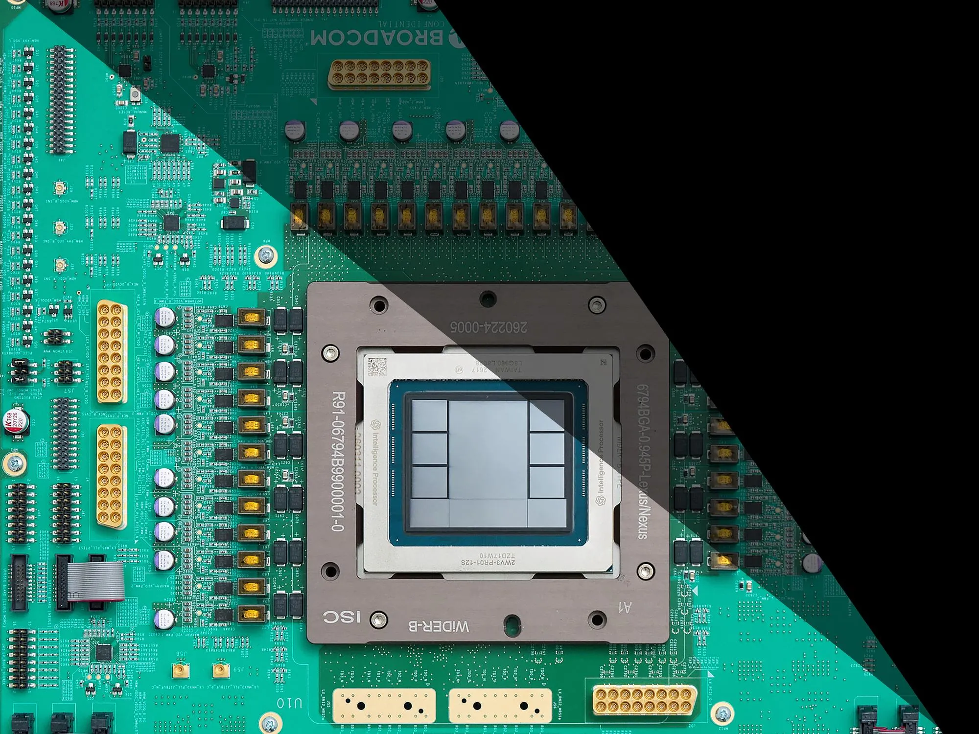
On 25 August, OpenAI fully unveiled Jalapeño, the company’s debut AI accelerator chip. Jalapeño delivers up to 13.4 petaflops of 4-bit compute and accesses 232 gigabytes of the most advanced memory available, linking to it at a blazing 15.4 terabytes per second. Benchmarks cited by OpenAI show that Jalapeño can reduce end-to-end latency (the time between prompt to last token) by up to 3.6 times when compared to Nvidia’s GB300—a chip the company currently relies on—and do so while consuming less power.
Whether these figures translate into real-world gains once Jalapeño enters widespread service in OpenAI’s inference fleet remains to be seen, but performance is only half the story. The other half is how the chip was designed—a process which, as you might expect, was accelerated by OpenAI’s large language models (LLMs). Jalapeño moved from first architecture concept to first silicon in under 20 months. Only nine months separated the first RTL—the register-transfer level code defining the chip’s logic—from tape-out, when the finished design goes to manufacturing.
That’s a rapid timeline, yet experts believe it could soon look slow as LLMs improve and become more deeply integrated into chip design tools. OpenAI, unsurprisingly, is bullish about the opportunities. “The models are giving superpowers to our engineers,” says Richard Ho, vice president of hardware at OpenAI. “Our engineers are still driving the work. They’re still the final arbiter of what’s going on. But they can do things a lot faster. They can explore a lot more paths.”
Ho says the group that designed Jalapeño averaged fewer than 100 people over the course of the project and continues to stand at roughly 100 today as the team pursues second and third-generation designs.
Source link