Lowering operating voltage is a key to SoC power optimization. In advanced FinFET processes at ~0.4–0.5V, it can also start to become a design risk. As edge AI pushes inference closer to endpoints, edge-AI SoCs must deliver real-time performance within tight energy and thermal limits. Traditional voltage scaling is no longer sufficient.
SoC designs are shifting towards much more extensive use of near-threshold operation to achieve step-function improvements in performance per watt. But this shift fundamentally changes how chips behave: delays increase non-linearly, variability grows significantly, and underpinning predictable operation becomes a critical enabler to minimizing power.
Design success in this operating regime depends heavily on the underlying quality, modeling accuracy, and integration of Foundation IP with EDA flows and silicon validation. Embedded memories, logic libraries, and I/Os must be selected carefully and any targeted optimization carried out and fully validated at an early stage—not treated as a possible downstream option.
Every SoC designer understands that lowering supply voltage reduces energy—but at near threshold voltages, it changes transistor behavior and challenges traditional design assumptions.
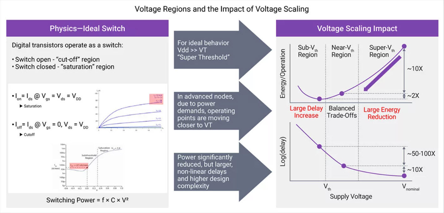
Fig. 1: Energy efficiency improves at lower voltage, but delay and variability increase sharply near threshold.
As shown in Figure 1, reducing voltage lowers energy per operation, but comes with significant trade-offs: delay grows rapidly, variability increases, and noise margins shrink.
Voltage scaling is no longer an isolated optimization—it introduces tightly coupled challenges across the entire design stack.
Meeting power targets at ultra-low voltage is not sufficient; designs must achieve this predictably and without introducing additional silicon risk.
Source link