Power delivery is now a significant performance limiter in data center chips. The demands of AI and high-performance computing chips running near 0.7 V for a 600W GPU are forcing current to rise to 1,000 amps and beyond, compounding resistive losses and voltage droop across the PDN. Multi-chiplet constructions only compound these issues by further increasing current density and signal congestion.
To solve these challenges, designers are turning to vertical power delivery networks, where the voltage regulator modules are relocated much closer to the processors from their position on the device periphery — to the PCB landside (under the PCB), inside the accelerator package, or inside the silicon interposer. Together with the growing customization of AI accelerator modules, there are many approaches on offer with varying design and manufacturing complexity.
The vertical PDN trend began nearly a decade ago with the integration of backside power delivery networks (BPDNs) on the wafer backside, enabling fine-tuned power delivery more directly to the transistors while reducing IR drop across the tens of interconnect levels on-chip. That approach is being extended with increasingly sophisticated on-die decoupling capacitors (DCaps) formed in deep trenches as part of the BPDN. While this addresses high-frequency decoupling at the chip level, recent changes inside packages, interposers, substrates, and across data center racks are becoming just as important.
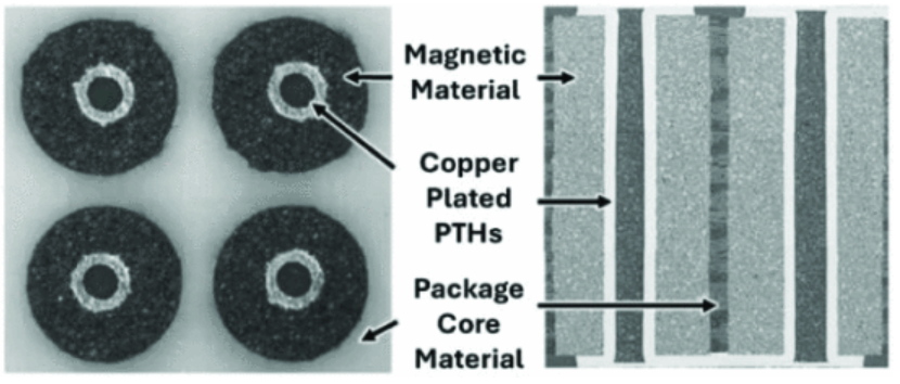
Add to that recent developments in the design of compact passive devices, like high-performance inductors, and new architectural solutions become possible, moving the VRMs and DC-DC converters into the interposer or package.
Source link