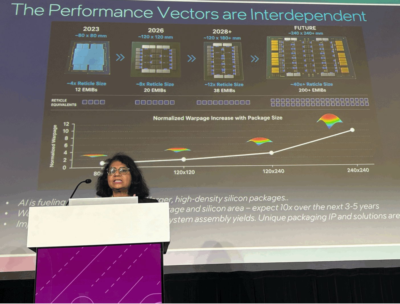
As demand for AI power and performance grows, chip designs increasingly involve 3D stacking, chiplets, and heterogeneous integration within a single package.
In a virtuous cycle, EDA tool vendors are leveraging advanced chips to simulate multi-physics challenges in a single tool instead of running individual solvers. Agentic AI is adding another layer of analysis to enable faster design exploration and automate various tasks. However, a few speed bumps remain due to the rapid progression of chip technology.
One challenge is that HPC/AI chip design must be considered across compute, memory, interconnect, power, and thermal constraints. “Today, nearly every AI accelerator has a process threshold where the hardest problems no longer live inside the chip. They live at the system boundaries,” said Artour Levin, vice president of AI silicon engineering at Microsoft.[1] “A standalone chip is not very beneficial for AI because very few things can be run on a single chip. You really need to look at the system level, and if you look at the history of EDA tools when they started, 30 or 40 years ago, it’s natural that EDA tools were designed to design chips, not a system.”
The chip-to-system threshold is where customers are facing challenges. “The design toolchain grew up around clean abstraction boundaries — cell, block, chip — with physics handled as episodic, domain-by-domain validation at the end,” said Hardik Kabaria, CEO and co-founder of Vinci . “That operating model worked when the hardest problems stayed inside those boundaries. It breaks when heat, stress, and electrical behavior move across the entire physical stack, because the physics insight arrives after the decisions that needed it have already been made.
Source link